For single-ended circuits, due to its load terminal directly or indirectly connected to VDD, which will inevitably bring the noise brought by the current source, this noise is called "common-mode interference", with this interference output signal reflected in the frequency domain will be spurious, in order to eliminate this interference, so many circuits will be used in the "differential pair".
And single-ended circuit bias voltage is similar to the bias voltage of the differential signal is called "common mode level", for the input differential signal, it is called the input common mode level, for the output is called the common mode level of the output, which is defined as the difference between the two junction potentials, and the two junction potentials with respect to a fixed potential equal in size and opposite in direction. In the differential signal, the center of the fixed potential is called "common mode level".

For actual differential amplification circuits, a current source is connected to the source common of the differential pair, as shown below:
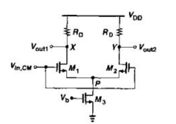
We all know that the MOS tube working in the saturation region, the drain current will change with the gate voltage changes, and use a constant current source to do the tail current, you can ensure that the two branches of the current flowing to the P point is the same, and because of the symmetry of the two branches, so their currents are respectively 1/2 of the tail current, and does not change with the change of Vin, CM, the role of which is to inhibit the input common-mode level of the changes on the M1 and M2 tubes. operation and output level of M1 and M2 tubes.
By studying the variation of Vout1-Vout2 with the variation of Vin1-Vin2, we can get the input-output characteristics of the differential pair as follows
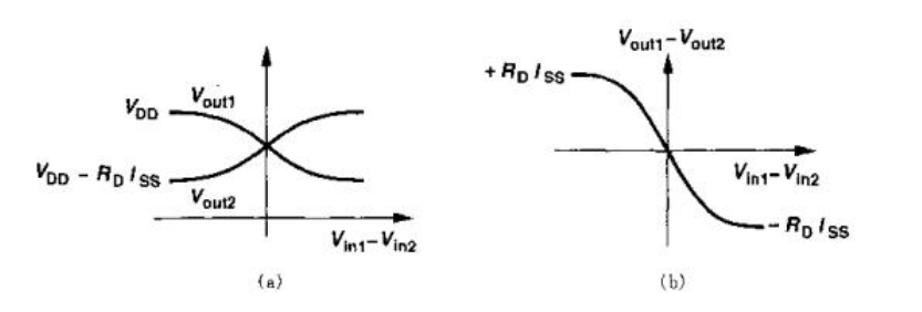
From Fig. (b), we can see that when Vin1-Vin2=0, the small signal gain (i.e., slope) is the largest, so it makes Vin1 and Vin2 in the same bias potential, and then the small signal can realize the amplification of the signal. The maximum and minimum levels of the large signal output are VDD and VDD-RD*Iss, and the small signal output ranges from -RD*Iss to +RD*Iss.
Summary:
(1) The differential amplifier circuit eliminates common mode interference and amplifies the signal by phase subtraction of the inverted signal.
(2) With the addition of the tail current, the bias will not change with the common mode level, which makes for a simpler bias circuit and higher output linearity.
(3) There are drawbacks to this construction, i.e. there is an increase in chip area and power consumption, but it is definitely worth every penny!
Perceptive Components Limited offers the widest selection of electronic components.
For more exciting articles, please click perceptive-ic.com.