Simply put, the processor manufacturing process can be roughly divided into sand raw material (quartz), silicon ingot, wafer, photolithography (lithography), etching, ion implantation, metal deposition, metal layer, interconnect, wafer test and There are many steps such as cutting, core packaging, grade testing, packaging and listing, and each step contains more detailed processes.
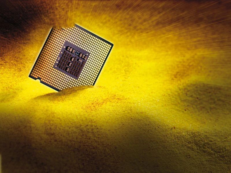
1: The central processing unit (CPU) is a very large-scale integrated circuit, which is the computing core and control core of a computer. Its function is mainly to interpret computer instructions and process data in computer software, which is one of the few items that cannot be copied so far. Of course, the manufacturing process of the CPU also represents the highest level of technological development in the world today.
2: Silicon is the second most abundant element in the earth's crust. Sand contains 25% silicon, which is the second most element in the earth's crust. After oxidation, it becomes silicon dioxide. In sand, especially in quartz, silicon dioxide The content is very high, which is the basis for manufacturing semiconductors.
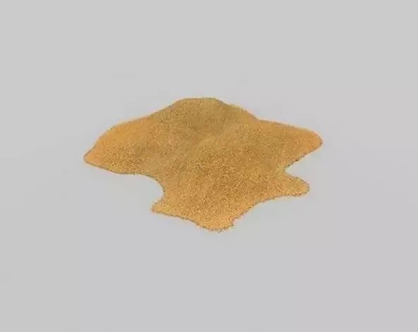
3: After the raw material sand is purchased, the silicon in it is separated, the excess material is discarded, and then purified through multiple steps to finally reach the quality that meets the requirements of semiconductor manufacturing. This is the so-called electronic grade silicon. Its purity is so great that only one out of every billion silicon atoms is non-compliant.
4: A single crystal of electronic-grade silicon that has been cast into an ingot weighs about 100 kilograms, and the purity of silicon reaches 99.9999%.
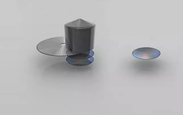
5: After the silicon ingot is cast, it will enter the cutting stage. The whole silicon ingot will be cut into discs one by one, which is what we commonly call wafers. In this way, the cut out is very thin, and then the wafer will be processed. Polished to perfection, the finish is as smooth as a mirror.
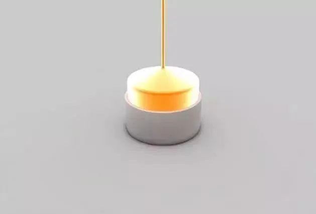
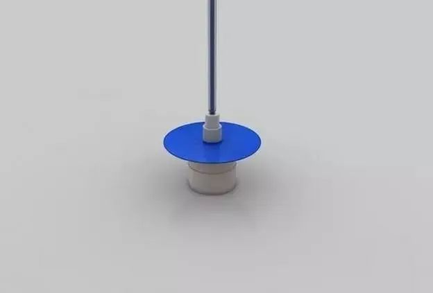
6: The blue liquid is coated on the wafer, which is similar to the photoresist when taking pictures with film. The wafer is constantly rotating to make it spread the liquid evenly on the wafer, and the coating is also very thin.
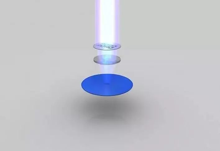
7: Irradiating the wafer with UV light. The ultraviolet light first passes through a "baffle" with a "pattern", whose function is to block part of the light and make the light shine on the wafer in a specific shape. The middle lens is used to focus the light into a small area. When ultraviolet light is irradiated on the photosensitive material, a chemical reaction similar to that of photosensitive film occurs, making the photosensitive material soluble. In this way, the "pattern" on the "baffle", which is actually the layout shape of the microcircuit, is "photocopied" on the wafer.
8: The transistor is equivalent to a switch, controlling the direction of the current. A transistor is the basic building block of a CPU. The current process can produce 300,000 transistors in an area the size of a pinhead.
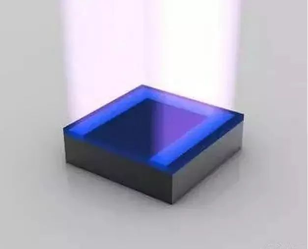
9: The photoresist exposed to ultraviolet rays during the photolithography process is dissolved, and the pattern left after removal is consistent with that on the mask. Photolithography is then performed, and the exposed parts are washed away.
10: Reapply the blue photoresist (blue) again and get ready for the next step. The blue part in the figure is the part protected by photosensitive material.
11: Ion implantation, that is, bombarding the silicon wafer in the exposed area with ions, and changing the conductivity of the silicon in these areas by impacting the implanted silicon wafer with ions. The ions need to hit the wafer surface at a very high speed, and after being accelerated by the electric field The speed of ions can reach 300,000 kilometers per hour.
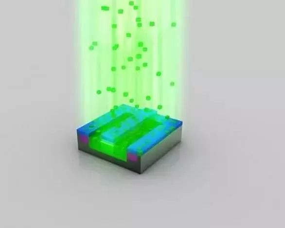
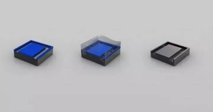
12: After ion implantation, the photoresist layer will be removed, and the material in the green part will be doped with late atoms.
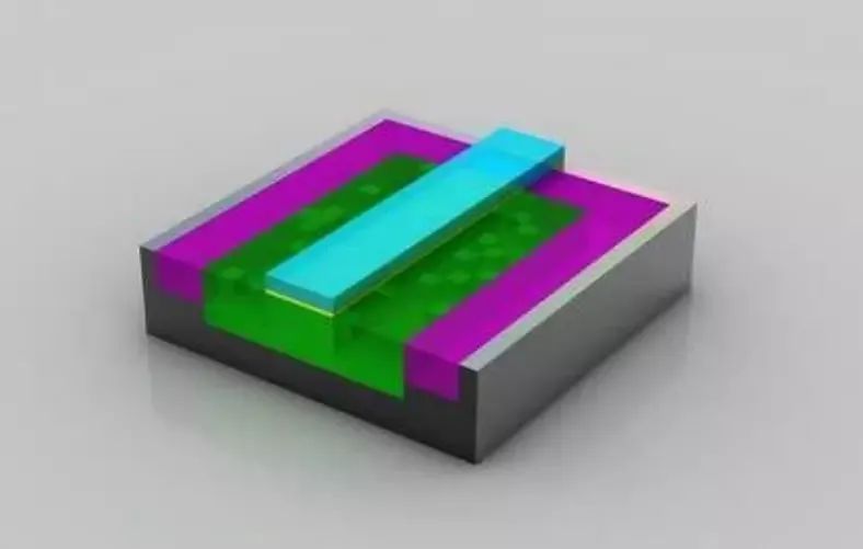
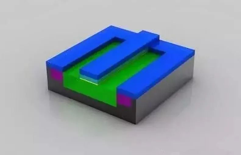
13: At this point the transistor is almost complete, the magenta surface of the transistor is the insulating layer, and there are three holes in it, these three holes will be used to fill the copper to connect to other transistors.

14: At the stage where the wafer is placed in the copper sulfate solution, the deposition of copper ions to the transistor is called electroplating. The free copper ions go to the positive terminal (anode) and negative terminal (cathode) of the wafer respectively.

15: The excess copper is polished away, leaving a very thin layer of copper.
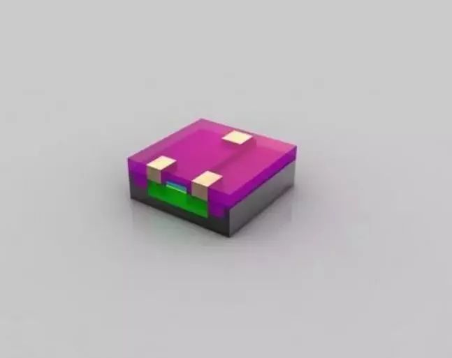
16: Multi-metal layers are the interconnection of various transistors. Although the computer chip looks very flat, it may actually have more than 20 layers, forming a complex circuit.

17: In this part, the wafer is prepared to establish the first functional test, enter each single chip in the test mode at this stage, and monitor the response of the comparison chip, and then discard the defective core chip.

18: The wafer is cut into pieces, and each piece is a core of a processor.

19: This is a separated core, Core i7, cut by the previous process.

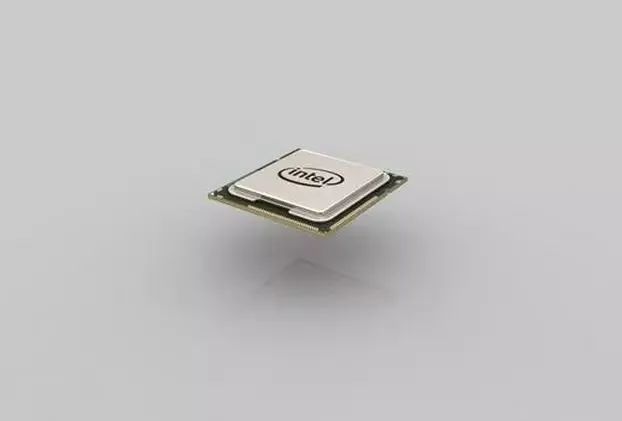
20: Stack the substrate (substrate pins), core, and heat sink together to form the processor we see.

21: Finally, each CPU will be tested. Based on the test results, the processors with the same capabilities are classified into one category, the highest operating frequency of the processors is determined by classification, and the price is determined according to specifications such as stability.