Without co-planarity, surfaces may not adhere properly. If no problem is found in the package, this can reduce yield or lead to reliability issues in the field. Identifying these issues requires various process steps, including various types of inspection and metrology, and the denser and smaller the bumps, the more intensive and time-consuming these processes become.
“As the I/O pitch within a die continues to decrease, the number of bumps required per die increases. In addition, the bump size continues to decrease,” said Doug Scott, vice president of wafer services at Amkor. “In some cases, there may be more than 5,000 bumps per chip. This requires each bump to be the same size and shape to ensure proper downstream assembly. A missing or misshapen bump will result in assembly failures and yield losses.”
There are other challenges, especially as the chips contained in these packages become more heterogeneous. "Total power at new nodes is typically still going up, driving customers to use mixed bump pitch and bump diameter for chip designs," said Mike Kelly, vice president of advanced packaging development and integration at Amkor. "This requires higher-end plating tools and often Slower plating times and an incentive to minimize cost impact. Our customers are mostly concerned with total current, which is mostly an electromigration issue, but it's also delivering a finer grid of current to new silicon nodes - 3nm in particular, but also starting at 5nm. This means more bumps on finer pitch, potentially facing more plating as bump pitch and bump diameter change across the chip challenge."
Structure
Bumps are simple solder balls, typically between 75µm and 200µm in diameter. They can be formed by electroplating or direct placement. "Both processes are well understood, well optimized, and successful in high volume manufacturing," Scott said. “It is also possible to use screen printing to make solder joints, but there are yield/solder voiding issues. Proper design between bump die and substrate/end PCB can significantly reduce failure points.”
The bumps are implanted on the IC in a flip-chip process - technically, a controlled collapse chip connection or C4. Once the chip is fabricated on the wafer, a metallized pad is placed on top of it and the bumps are attached. Then, cut the chips and flip them over.
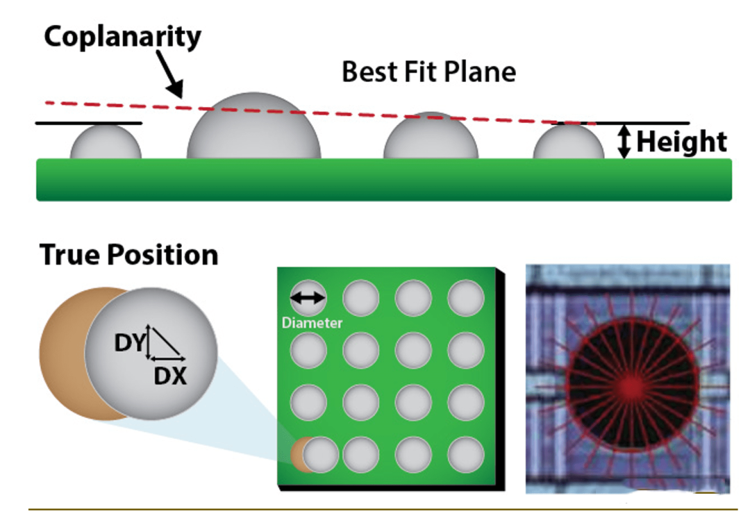
Ideally, the bumps align perfectly with the connectors on other components. This is where problems often occur, either due to defects in the bumps themselves, or due to substrate warpage that prevents the bumps from aligning properly.
"Interconnections between chiplets rely on microbumps with solder thicknesses less than 10 microns," said Marc Swinnen, director of product marketing for Ansys' Semiconductor Division. “The solder volume of microbumps is about two orders of magnitude smaller than conventional flip-chip joints. This means that even slight bending or warping of the interposer substrate presents a significant reliability risk. In addition, these microbumps are required to Together they carry hundreds of watts of power. Any localized overheating can lead to thermal failure of these tiny structures.”
“You have a variety of materials, different substrates, and they all have different coefficients of thermal expansion,” said Frank Chen, director of application and product management at Bruker Nano Surface & Metrology. "When you have these mismatches, some things cool faster than others, and you get a lot of warping and stress that you can't completely eliminate. The reality is, it's hard to get a flat surface."
In many cases, this warpage is so small that it even requires special equipment to detect.
"What really challenges people are the three main types of bump defects -- bridging, non-wetting, and voiding," Chen said. “But there are also metrology-type issues, such as die placement errors, including die shift and rotation. Another issue associated with die attach is pressure. The typical process is to apply pressure and heat to connect the die, but due to pressure or heat The distribution is uneven and you might get some tilt or warping."
Voids can make the solder connection interface look like Swiss cheese and are the source of thermal and power problems. "Voids are known to be very poor conductors of heat and interfere with the transfer of heat away from the component," said Anders Schmidt, applications engineer at Palomar Technologies. "Because the component does not dissipate heat well, its current-carrying capacity decreases, resulting in inefficient power utilization. ."
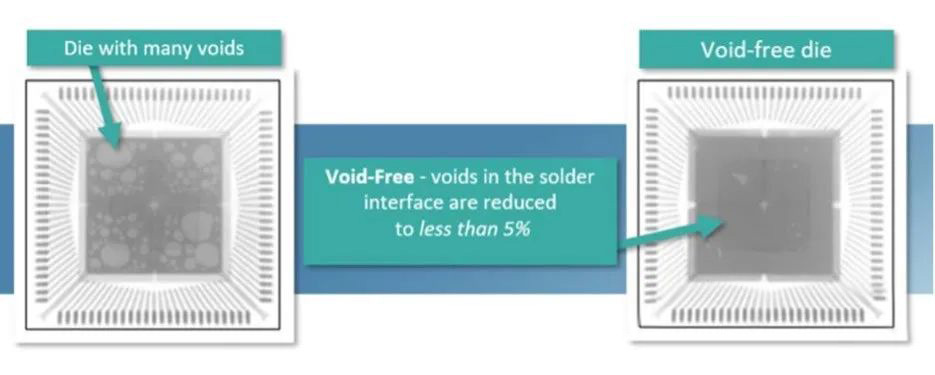
In the worst case, the voids can lead to chip cracking. The solution, according to Palomar, is to use eutectic bonding, where the melting point is lower than that of each individual material. This can be achieved using an intermediate metal layer. "During the bonding process, but during device operation, the melting point is very low, which is one of the key properties of eutectic bonding," Schmidt said.
Because solder bumps are metal, they also help with heat dissipation. "A reliable solder will work with the package to dissipate heat generated internally, maintain long-term functionality at operating temperatures, and withstand shocks caused by environmental conditions or power cycling."
Evolving Materials
First introduced by IBM in 1964, bump designs became popular as components shrunk because they allowed more I/O connections in the same space as wire bonds, while also reducing thermal resistance and inductance.
Initially, the bumps were made of a tin-lead (SnPb) alloy. In keeping with current environmental concerns, they are now more often made of tin-silver-copper (SnAgCu or SAC) alloys. Given that there can be thousands of bumps on a single component, this transformation has important implications for environmental audits, as material audits can be down to the atomic level.
Alan Porter, vice president of electronics and semiconductor strategy at Siemens Digital Industries Software, said: "If your product contains different materials, each of which may contain a lead atom, when you aggregate these materials in Together, at some point, lead becomes measurable and important."
Currently, there are many bump and substrate configurations from different suppliers, all designed to optimize electrical connections for better performance. [2] Advances in underfill materials, electrically insulating adhesive layers in flip chips (not to be confused with "underfill" [3]) are also improving efficiency.
Among the many options are pure copper "microbumps" ranging in diameter from 20µm to 25µm, which offer the same advantages of wire bonding over bumps compared to larger bumps. As pitches get smaller, starting more than a decade ago, many manufacturers started using "C2 bumps," which are pillar-like microbump structures with tin-silver (SnAg) contacts on top.
These SnAg tips offer reliability advantages. But subtle differences in ingredients can affect the bump's behavior. According to Fisher Instruments, "Solder bumps with more than 3% silver performed better in thermal fatigue testing and were more resistant to shear plastic deformation, while alloys with lower silver content (about 1%) showed excellent performance. ductility and therefore better fatigue resistance under severe strain conditions. In addition, as little as 0.5% copper can reduce the dissolution behavior of the copper in the substrate, thereby improving solderability.”
One of the fundamental manufacturing challenges here is maintaining the proper balance of material composition. This creates a significant opportunity for X-ray inspection, which has been on the sidelines for many years. X-rays can be used to determine material composition, such as alloys in interconnects or contamination in bumps. Additionally, it can help identify structural defects.
The disadvantage of X-ray inspection is that it is fast and is often combined with optical inspection. But as interest has grown, the speed of the technology has increased significantly.
"A voided bump doesn't absorb as many X-rays as a solid sphere," Chen explained. "Because there's a hole in it, the air doesn't really attenuate the X-rays. In the case where it's a solid sphere, you get more absorption. When you look at the camera, then you see there's a black spot because It absorbs all the X-rays, so you don't see the light there - you see more of it than the one with the hole. It's not completely transparent, but it looks a little light. So we're Look at the difference in image contrast and absorption, then compare what is known to be good and what is known to be bad to see which is bad."
Process Steps
The current demand for smaller processors, more I/O in smaller footprints, and smaller packages has also prompted OSATs to rethink process sequences. “Once rigorous back-end processes, such as packaging, are now moving more to the front-end,” said John Hoffman, computer vision engineering manager at CyberOptics. “The industry tends to refer to these processes as intermediate processes, especially when fab or packaging factory when performing these steps.
Since the reliability of the final product depends on the precise alignment of the bumps, inspections must be performed in advance, which forces further adjustments. "This requires preparing the sample in some way," Chen said. "And these testing protocols take time to design."
Others agree. “Today, when it comes to backend/package inspection, we don’t have a clear link between the inspection and the assembly process,” said Olivier Dupont, product marketing manager for KLA’s ICOS division, in a recent interview. "This is an area of future development that needs to be built. As many have observed, the growth of advanced packaging continues. It has to invest in that development."
zoom
As the size of chips and packages continues to shrink, bump technology is being replaced by hybrid bonding.
Today, the smallest pitch and diameter in production are around 20µm pitch and 10µm diameter. "Some customers are trying to do hybrid bonding after 20-micron pitch, 10-micron diameter, and some of them are trying to move to hybrid bonding after 5-micron diameter, 10-micron pitch," said Woo Young Han, manager of applications engineering at Onto Innovation. "That's the limit of our bump today. Anything smaller than that would be a direct copper-to-copper surface bond."
One area of concern is the wafer edge. "A surface roll-off of a few nanometers could disrupt the hybrid bonding between wafers," Han said. “Many of our customers want to inspect incomplete chips at the edge of the wafer. While it won’t be used, any defect on part of the die can disrupt the entire process. Therefore, many inspection companies are looking into deep learning or human-based Smart way to inspect part molds.”
Jean Trewhella, post-fab director at GlobalFoundries, said that while these issues are often the top concerns, there is another lesser-known issue in the fabrication of micropillar bumps. "Making the micropillars wasn't the biggest challenge," she said. "Instead, when you try to test them or connect them to something else, you don't get any extra foreign material. It's not like a clean room where we do collisions."
Also, the tests themselves can sometimes cause damage. "We have to physically touch that bump or ball, so we have to make sure that the Pogo pin technology we're using doesn't cause too much damage," Amkor's Harris said. "Also, we have to make sure our environment is clean. If you have a connection between a ball and a dirty power source, you usually need to increase the voltage or current when testing to meet a certain level. There is resistance in that path. If that is Carbon-based material, it can burn and damage the socket, which can damage the device.”
In Conclusion
Amkor's Scott is optimistic that these issues can be resolved. "As the bump pitch decreases, new photoresist materials and exposure equipment are required," he said. “We need to continue investing in better equipment and materials, as well as increasing statistical process control and metrology. In addition, it is important to understand the end application requirements to ensure that the design is suitable to meet the service life requirements.”
He's not alone in being optimistic. "When you add up all these probabilities, given the number of pillars and everything else, PPM is no longer uncommon," said John Carulli, a researcher at the Post Fab Test Development Center at GlobalFoundries. "As I benchmark and talk to various peers across the chain, these are questions. There aren't many solutions out there. But a lot of smart people are doing a lot of good work on this."
Addressing these issues could bring enormous benefits and opportunities. Chip Greely, vice president of engineering at Promex Industries, said: “Higher throughput means lower cost, more consistent equipment doing the same thing in time/overtime, so costs should come down.

