Wide-bandwidth (WBG) semiconductors such as silicon carbide (SiC) and gallium nitride (GaN) are enabling higher efficiency, smaller size power conversion solutions for next-generation photovoltaic (PV) and energy storage systems (ESS). In this article, we will highlight examples of such products offered by Infineon Technologies and Toshiba.
Strong Growth in Photovoltaic Installations and Power Generation
The 2050 climate change goal of net-zero greenhouse gas emissions is driving the adoption of renewable energy production in many countries. The combination of improved efficiency and reliability of photovoltaic (PV) panels, cost reductions and government subsidies is driving significant growth in solar power generation. cumulative installed PV capacity exceeds 1TW in 2022, with 240GW of new capacity added during the year. This accounts for two-thirds of the new installed renewable energy capacity in 2022. The cumulative annual growth rate is expected to be around 20% in the coming years. It is estimated that wind and solar will account for about two-thirds of all energy production by 2050.
Trends in PV and ESS Power Conversion
For residential use, PV output is typically less than 20kW with a maximum DC voltage of 600V and a typical single-phase output of 110/230VAC.
Currently, utility-scale PV is typically rated at 1,000 V. Lower ohmic losses and the resulting improved end-to-end efficiency, combined with fewer parallel strings to reduce installation costs, are driving an increase in this voltage from 1,000 V to 1,500 V. Grid-connected utility generators can have power outputs ranging from a few hundred kilowatts (kW) to several megawatts (MW).
ESS systems expand accordingly, with typical residential wall-mounted units ranging from 3kW to 20kW, and battery voltages rising to the 450V range. Commercial and utility ESS installations range up to the megawatt level.
The method of connecting the ESS can be either AC-coupled (in which the battery is connected to the grid via a combination of DC/DC and DC/AC conversions, and then connected to the grid) or DC-coupled (in which the DC PV power supply is connected to the battery via a DC/DC converter). Such hybrid inverters with a built-in ESS function avoid unnecessary power conversion. These converters must be bi-directional to capture and absorb battery energy based on supply and demand.
With the increasing popularity of electric vehicles, EV batteries can be used as an energy source in a vehicle-to-home configuration. Here, the EV battery can be DC coupled to a photovoltaic hybrid inverter via a bidirectional DC/DC converter or AC coupled to the grid via an on-board or off-board bidirectional DC/AC inverter.
A variety of converter designs are used here, each with its own advantages.CLLC and dual active bridge (DAB) are common topologies for bi-directional isolated DC/DC converters, where isolation is required between the low voltage (e.g., 48V for the battery or PV power supply) and the high voltage dc output (to power the inverter, e.g., 400V). Non-isolated step-up DC/DC inverters can be used when low voltage is not available, such as the output of a larger string solar system that outputs 600V.
Transformerless bi-directional DC/AC converter designs - such as the High Efficiency and Reliable Inverter Concept (HERIC) or Multilevel Active Neutral Converter (ANPC) - are becoming increasingly popular due to increased efficiency and reduced system cost, size and weight.
HERIC inverters can be used in single-phase string inverters with outputs of up to a few kilowatts, while ANPCs can be used in central inverters with outputs ranging from hundreds of kilowatts to several megawatts. Multilevel ANPCs allow the use of devices with lower voltage ratings (Vbus÷(n-1), where Vbus is the full bus voltage and n is the number of levels) and also reduce the voltage transitions (dv/dt) during the conversion period, which reduces electromagnetic interference.
WBG Devices for PV and ESS Power Conversion
WBG devices offer many advantages over conventional Si devices in PV and ESS bidirectional DC/DC and DC/AC converter designs. Higher switching frequency reduces system size and improves efficiency. Reduced losses can make cooling requirements simpler. GaN devices can also provide unique bi-directional functionality for simpler AC switching topologies, reducing device count by a factor of four.
Figure 1 shows the scope for SiC and GaN devices in solar and ESS applications. SiC is well suited to replace Si devices in the higher power and higher voltage arena, with device ratings ranging from 1,200 V to 3,300 V. Fast-switching GaN devices rated at 650 V or less are well suited for individual PV microinverters and DC/DC converter applications.

Figure 1: SiC and GaN application space in solar and ESS systems
As shown in Figure 2, CoolSiC and CoolGaN devices from Infineon offer several advantages over conventional Si devices.
SiC improves the RDS(on) characteristics over temperature.GaN HEMTs have lower output and gate charges (Qoss and Qg, respectively), resulting in the lowest switching losses. GaN's lower Qoss can be used to reduce dead time and lower the RMS factor in soft-switching CLLC topologies.

Figure 2: SiC and GaN comparisons in on-state resistance, output charge behavior with drain voltage and gate charge versus gate voltage,
compared with superjunction Si MOSFET devices of similar voltage and RDS(on) ratings
These advantages translate directly into improved converter efficiency. For example, when discharging a 56V ESS battery to a 400V bus, a DC/DC CLLC converter operating above the resonant frequency can achieve much lower reverse recovery losses on the secondary-side high-voltage switches that are performing synchronous rectification. The Miller gate charge (Qgd) on the primary FETs of a DAB converter will be much lower, resulting in much lower Eoff losses on the primary-side FET.
The body diode's ability to withstand inrush currents well above the device's nominal current rating may be another key advantage of the SiC MOSFET's ability to achieve bi-directional power conversion. SiC-based converters can operate at several times the switching frequency of similarly rated Si IGBTs while still having small or comparable losses, saving on the size of the system's magnetic components, which in turn reduces size and cost. Infineon's discrete CoolSiC device products are rated from 650V to 2,000V and are suitable for both hard-switching and resonant switching topologies.
At PCIM 2023, Toshiba introduced SiC MOSFETs with embedded Schottky barrier diodes (SBDs) rated at 2,200 V. The devices are packaged as dual SiC MOSFET modules. This rating allows the use of two-level inverters in 1,500V PV applications. They have fewer switching stages than three-level topologies and are therefore smaller and lighter. The devices, rated at 2,200V, follow the same RDS(on) versus Vds relationship as previous SiC MOSFETs rated at 1,700V and 3,300V.
SiC MOSFETs may be affected by the growth of base plane defects during the forward conduction phase of their built-in body diode. This can lead to increased RDS(on) and reduced reliability. Unipolar SBD conduction effectively avoids this bipolar conduction phase, thereby improving reliability. The use of SBDs also reduces dead time losses in the converter due to their lower forward conduction voltage.
One of the problems in photovoltaic applications is cosmic ray degradation and failure. A study has shown that the single-event burnout failure rate due to terrestrial neutron exposure is a function of the VDS/VAVAL ratio, where VDC is the rated voltage of the device and VAVAL is its avalanche onset voltage. For devices with a VDS/VAVAL of 0.5 or less, the real-time failure rate is much lower (<1) in parts per billion. This ratio can be adjusted by epitaxial/drift layer optimization. As shown in
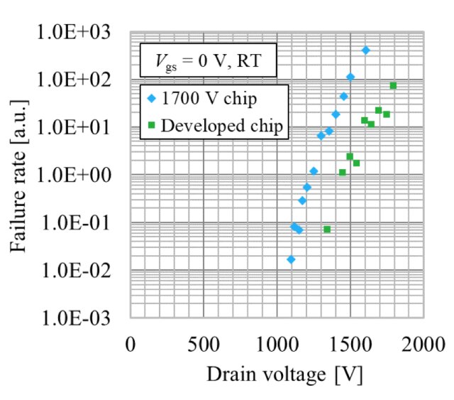
Figure 3: Neutron irradiation failure rate of the Toshiba 2,200-V SiC MOSFET (shown in green), versus the existing 1,700-V device
Figure 3, these 2,200V SiC MOSFETs have an order of magnitude higher failure rate under white neutron irradiation (shown in green) compared to 1,700V MOSFETs.
High-temperature reverse bias testing of these 2,200V MOSFETs at full rated VDS of 150°C showed that key DC parameters-such as threshold voltage Vth, RDS(on), and drain leakage-at a 2,000-hour stress intervals showed a change of less than 5 percent.
They compared the switching performance of three-level inverters using 1,200V and 1,700V Si IGBTs (operating at 3.9kHz) with two-level inverters using these 2,200V SiC MOSFETs (operating at 7.8kHz). This was done at 1,200 V, 200 A and 125°C. The power consumption of the 2,200V converter was significantly reduced by 37%, even at the higher frequency.
Both residential and utility-scale PV can benefit from the use of WBG power converters and ESS solutions. Microinverters and single-phase string inverters can benefit from GaN's low-loss, high switching performance, which greatly increases power density and simplifies converter topologies. High-power hybrid inverters and three-phase central inverters for utilities can also benefit from SiC devices, which outperform silicon-based devices in terms of power loss, high-temperature performance and power density.
If you like this article, click into perceptive-ic.com to see more.