Features:
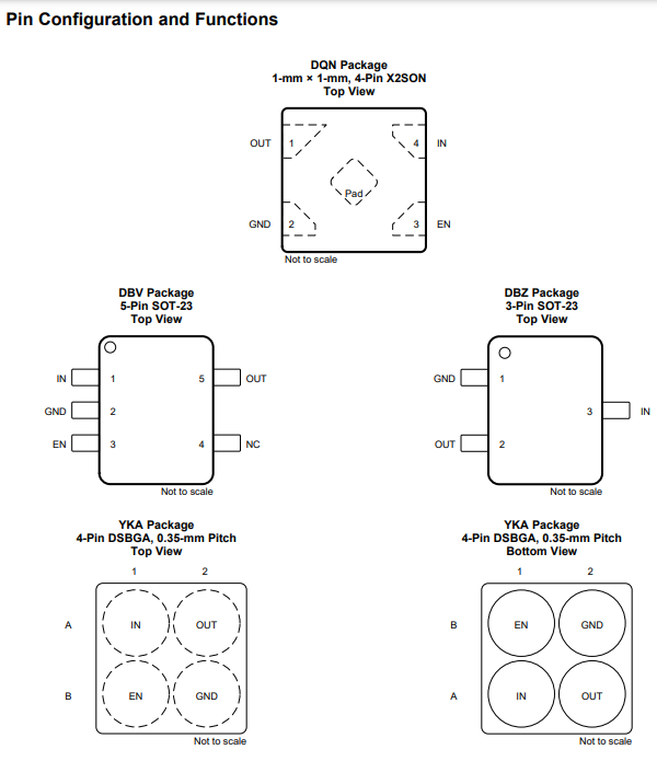
1• Ultralow IQ: 1 µA (typ), 3 µA (max) – IGND: 6 µA (typ) at 200 mA • Excellent transient response • Packages: – 1.0-mm × 1.0-mm X2SON (4) – 0.65-mm × 0.65-mm DSBGA (4) – SOT-23 (5) – SOT-23 (3) • Input voltage range: 1.4 V to 5.5 V • Output accuracy: 1% typical, 3% maximum • Available in fixed-output voltage: – 0.8 V to 3.3 V • Very low dropout: – 235 mV (max) at 200 mA (3.3 VOUT) • Active output discharge • Foldback current limit • Stable with a 0.47-µF or larger capacitor
Applications:
• Wearable electronics • Ultrabooks, tablets, E-readers • Always-on power supplies • Set-top boxes • Gaming controllers, remote controls, toys, drones • Wireless handsets and smart phones • Portable and battery-powered equipment
Description:
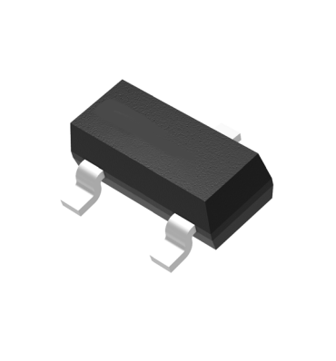
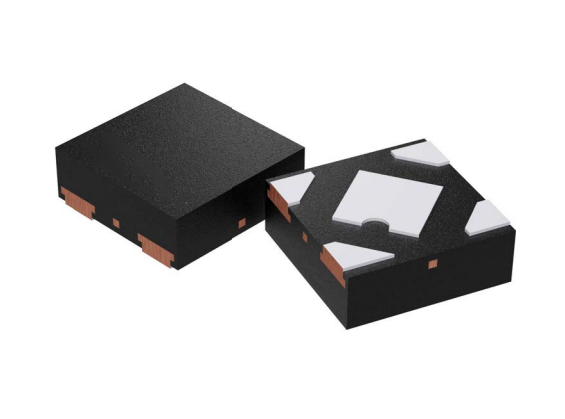
The TPS7A05 is an ultra-small, low quiescent current low-dropout regulator (LDO) that can source 200 mA with excellent transient performance. This device has an output range of 0.8 V to 3.3 V with a typical 1% accuracy. The TPS7A05, with ultralow IQ (1 µA), consumes very-low quiescent current for extending battery life in battery-powered applications. The device can be operated from rechargeable Li-Ion batteries, Liprimary battery chemistries such as Li-SOCl2, LiMnO2, as well as two- or three-cell alkaline batteries. The TPS7A05 is available with an active pulldown circuit to quickly discharge the output when disabled. The TPS7A05 is fully specified for TJ = –40°C to +125°C operation, and is available in standard X2SON (DQN), SOT-23 (DBV and DBZ), and DSBGA (YKA) packages.
Overview:
The TPS7A05 is a ultra-low IQ linear voltage regulator that is optimized for excellent transient performance. These characteristics make the TPS7A05 ideal for most battery-powered applications. This low-dropout regulator (LDO) offers foldback current limit, shutdown, thermal protection, and optional active discharge.
Excellent Transient Response:
The device includes several innovative circuits to ensure excellent transient response. Dynamic biasing increases the IQ for a short duration during transients to extend the closed-loop bandwidth and improve the device response time during transients. Adaptive biasing increases the IQ as the dc load current increases, extending the bandwidth of the control loop. The device response time across the output voltage range is constant because of the use of a buffered reference topology, which keeps the control loop in unity gain at any output voltage. These features give the device a wide loop bandwidth during transients that ensure excellent transient response while maintaining the device low IQ in steady-state conditions; see the Application and Implementation section for more details.
Active Discharge:
Devices with this option have an internal pulldown MOSFET that connects a 120-Ω resistor to ground when the device is disabled to actively discharge the output voltage. The active discharge circuit is activated when the device is disabled, in undervoltage lockout (UVLO), or in thermal shutdown.
The discharge time after disabling depends on the output capacitance (COUT) and the load resistance (RL) in parallel with the 120-Ω pulldown resistor. Equation 1 calculates the time constant:
Do not rely on the active discharge circuit for discharging a large amount of output capacitance after the input supply has collapsed because reverse current can flow from the output to the input. This reverse current flow can cause damage to the device. Limit reverse current to no more than 5% of the device-rated current.
Enable:
The enable pin for the device is active high. The output of the device is turned on when the enable pin voltage is greater than the EN pin logic high voltage, and the output of the device is turned off when the enable pin voltage is less than the EN pin logic low voltage. A voltage less than the EN pin logic low voltage on the enable pin disables all internal circuits. At the next turn-on, any voltage on the EN pin below the logic low voltage ensures a normal start-up waveform with start-up ramp rate control, provided there is enough time to discharge the output capacitance. If shutdown capability is not required, connect EN to IN. VEN must not exceed VIN.

Application Information:
(continued) If the EN pin is ramped down faster than 100 µs, the next startup may exhibit a delay time of up to 130 ms before the output ramps up with a normal soft-start startup. Figure 49 shows this delay.
Behavior When Transitioning From Dropout Into Regulation:
Some applications may have transients that place the device into dropout, especially as this device can be powered from a battery with high ESR. A typical application with these conditions is using a stack of two 1.55-V coin-cell batteries with an ESR of 30 Ω to create a 2.5-V rail and experiencing a load transient from 1 µA to 25 mA. This load transient causes the input supply to drop 750 mV, placing the device into dropout. The load transient saturates the output stage of the error amplifier when the pass element is driven fully on, making the pass element function like a resistor from VIN to VOUT. The error amplifier response time to this load transient is limited because the error amplifier must first recover from saturation and then place the pass element back into active mode. During this time VOUT overshoots because the pass element is functioning as a resistor from VIN to VOUT. This device uses a loop pulldown circuit to help mitigate the overshoot. If operating under these conditions, applying a higher dc load or increasing the output capacitance reduces the overshoot because these solutions provide a path to dissipate the excess charge.
