Overview
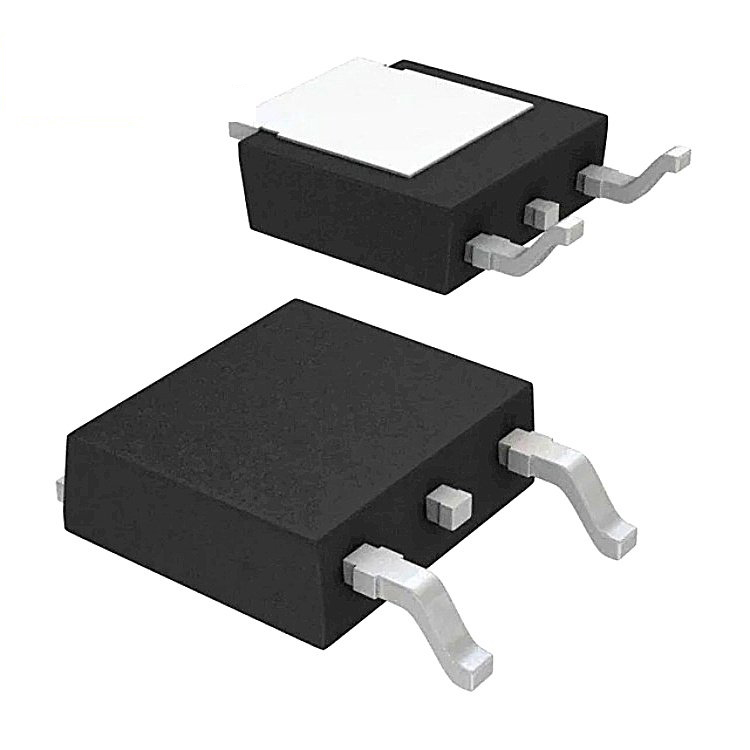
The SN74LVC1G17 device contains one Schmitt trigger buffer and performs the Boolean function Y = A. The device functions as an independent buffer, but because of Schmitt action, it will have different input threshold levels for a positive-going (VT+) and negative-going signals. The DPW package technology is a major breakthrough in IC packaging. Its tiny 0.64 mm square footprint saves significant board space over other package options while still retaining the traditional manufacturing friendly lead pitch of 0.5 mm. This device is fully specified for partial-power-down applications using Ioff. The Ioff circuitry disables the outputs, preventing damaging current backflow through the device when it is powered down.

Feature Description
• Wide operating voltage range.
– Operates From 1.65 V to 5.5 V.
• Allows Down voltage translation.
• Inputs accept voltages to 5.5 V.
• Ioff feature allows voltages on the inputs and outputs, when VCC is 0 V.

Application Information
The SN74LVC1G14 is a high drive CMOS device that can be used for a multitude of buffer type functions where the input is slow or noisy. It can produce 24 mA of drive current at 3.3 V making it Ideal for driving multiple outputs and good for high speed applications up to 100 MHz. The inputs are 5.5 V tolerant allowing it to translate down to VCC.

Layout Guidelines
1. When using multiple bit logic devices inputs should not ever float.
2. In many cases, functions or parts of functions of digital logic devices are unused, for example, when only two inputs of a triple-input AND gate are used or only 3 of the 4 buffer gates are used.
3. Such input terminals should not be left unconnected because the undefined voltages at the outside connections result in undefined operational states.
4. Specified below are the rules that must be observed under all circumstances.
5. All unused inputs of digital logic devices must be connected to a high or low bias to prevent them from floating.
6. The logic level that should be applied to any particular unused input depends on the function of the device.
7. Generally they will be tied to Gnd or Vcc whichever make more sense or is more convenient.
Mechanical, Packaging, and Orderable Information
The following pages include mechanical packaging and orderable information. This information is the most current data available for the designated devices. This data is subject to change without notice and revision of this document. For browser-based versions of this data sheet, refer to the left-hand navigation.