Wide bandgap (WBG) semiconductor devices such as silicon carbide (SiC) field-effect transistors (FETs) are known for their minimal static and dynamic losses. In addition to these attributes, the technology can withstand high pulsed currents, which proves particularly beneficial in applications such as solid-state circuit breakers. This article takes an in-depth look at the characteristics of SiC FETs, providing a comparative analysis with conventional silicon solutions.
WBG devices lead the ongoing quest to minimize semiconductor switching power losses, with SiC FETs taking center stage. Utilizing a common source and gate structure of SiC junction gate field effect transistors (JFETs) and co-packaged silicon metal-oxide-semiconductor field effect transistors (MOSFETs), these devices are normally-off devices with user-friendly gate drivers. Their impressive "quality factor" combination outperforms competing technologies, with a particular focus on on-resistance per unit chip area (R DS xA), a measure of low static and dynamic power consumption combined with cost-effectiveness. Despite their smaller die size (meaning more cells per wafer and lower device capacitance), SiC FETs have exceeded expectations by demonstrating enhanced temperature resistance and higher peak current capability. Let's look at the numbers.
SiC FET On-Resistance Performance
Quantifying the performance of the SiC FET, as exemplified by Qorvo's 750V rated UJ4SC075005L8S part, shows that the R DS xA value is 2.2 times better than that of a Gen 4 SiC MOSFET and remains constant over the entire temperature range. In fact, the device's on-resistance of 5.4 mΩ at 25 °C and 9.2 mΩ at 125 °C exceeds the V of silicon or SiC-MOSFETs rated at 600/650 and gallium nitride high electron mobility transistors (GaN HEMTs) in the same package by a factor of 4 to 10.
To achieve high current ratings with this ultra-low resistance, the example SiC FETs use silver-sintered die attach and advanced wafer thinning techniques to achieve a 0.1 °C/W thermal resistance from junction to case. In addition, the SiC devices have a maximum junction temperature of 175 °C, which means that a single device can handle 80 A continuously when connected to a simple 0.58 °C/W heatsink, with a junction temperature of 175 °C at an 85 °C ambient setting.
SiC FET Peak Current Ratings
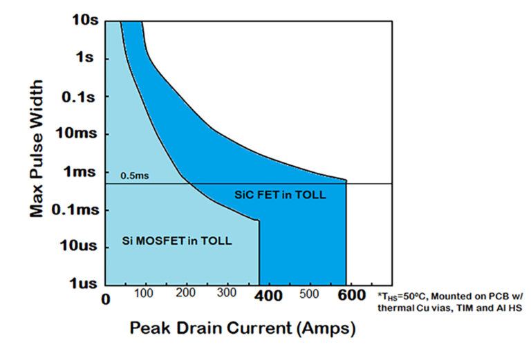
The maximum junction temperature (T J,Max ) value of a SiC device and its current rating are essentially determined by the package used. Although SiC has an inherent material capability to operate safely at temperatures in excess of 500 °C, the JFETs for common-source, common-gate SiC FETs are limited to a maximum temperature of 175 °C. This limitation still allows the SiC FETs to handle transient peak currents that are significantly higher than their sequential ratings during startup at lower temperatures. Transient thermal impedance plots for specific chips and packages (such as the SiC FET devices mentioned earlier) summarize these characteristics, as shown in Figure 1.
Figure 1: Transient thermal impedance of the SiC FET device vs pulse width and duty cycle.
For example, a single 100 µs pulse results in a transient junction temperature increase of about 0.015 °C per watt of power dissipation. at about 10 ms pulse duration, the junction-to-case thermal impedance approaches a steady-state value.
Figures 2 and 3 depict the actual impact of the example SiC FET devices. In each case, the device housing is soldered to a copper plane on the PCB and passes through a copper heat sink to a backside aluminum heat sink maintained at 50 °C, separated by an insulating thermal interface material (TIM). Figure 2 shows that the thermal resistance from junction to ambient can be greater than 1.2 o C/W, while the chip and TOLL package dictate a transient thermal response of less than about 1 ms. With this arrangement, the continuous current rating is 89 A, as shown in Figure 3, and the device can handle peak currents of up to 588 A in a single pulse for 500 µs before reaching T J,Max at 175 °C.
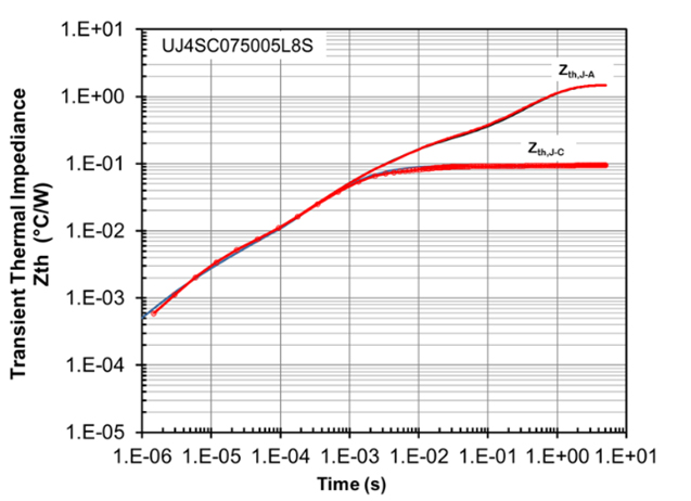
Figure 2: Modeled transient thermal impedance of the SiC FET device in a TOLL package when assembled on PCB with thermal vias, TIM, and Al heatsink.
Figure 3. Practical peak current capability of the Sic FET device for a TJ,Max of 175 °C.
SiC FETs and Si-MOSFETs
While SiC FETs show impressive results, a key question arises: How do they compare to Si-MOSFETs, which are commonly used in low-power solid-state circuit breakers? Current squared over time (I 2 t) ratings, a common measurement for devices that handle inrush current, provide a compelling comparison. The example SiC FET can withstand 588 A for 500 µs, while the Si-MOSFET is rated at about 200 A. The difference in "
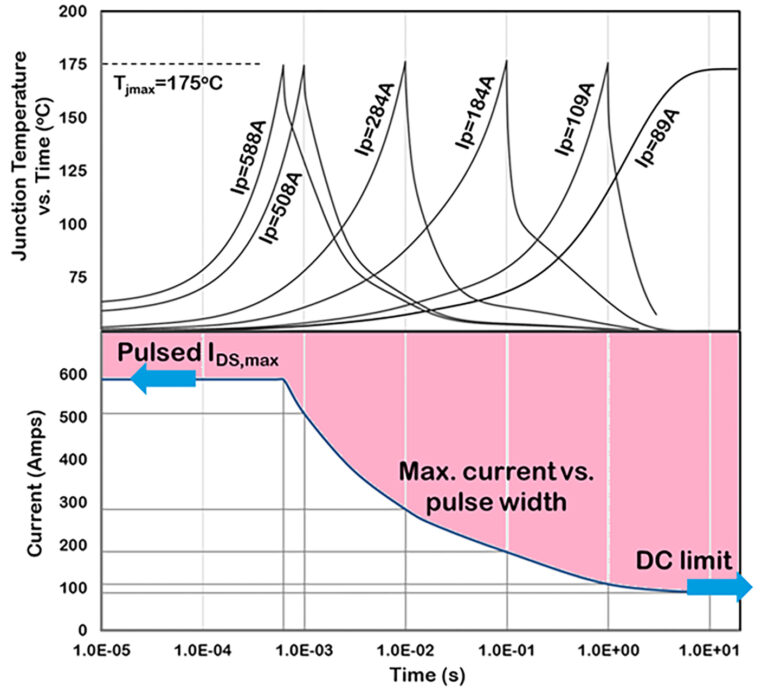
I 2 t" is a factor of 8.6, as shown in Figure 4.
Figure 4: Comparison of SiC FET and Si-MOSFET I2t ratings.
Additional Benefits of High Peak Current Ratings
In addition to the significant safety margins provided by SiC FETs under overload conditions, there are other advantages. SiC FETs have proven to be well suited for power conversion circuits with inductive loads where voltage overshoot is expected. These devices have strong avalanche capability and a 750V rating. In addition, on-board DC-DC converters in servers and similar applications, driven by data-intensive applications such as Artificial Intelligence (AI), Machine Learning (ML) and streaming media, increasingly require high peak power ratings in compact form factors.
These converters are often designed with the assumption that the junction temperature will be close to its maximum due to peak currents. Digital control, facilitated by PMBus™ sensors and predictive algorithms, provides junction temperature feedback, instructing the load to "throttle" as needed to prevent the switching junction from exceeding its absolute maximum. The ample margin provided by SiC FETs increases confidence in the reliability and longevity of the power system and has the potential to reduce the need for multiple parallel devices, resulting in cost and board area savings.
Designed to respond to high fault currents, solid-state circuit breakers can utilize SiC FETs and JFETs to achieve low dropout voltages, replacing insulated gate bipolar transistors (IGBTs), especially at lower current levels. The peak current rating of SiC FETs increases the robustness of these circuit breakers, allowing the overcurrent detection circuitry to have a longer delay before responding. This attribute makes the circuit breaker more immune to "nuisance" triggering.
Conclusion
Compact SiC FETs with peak current ratings in the hundreds of amps become ideal components for modern power conversion applications requiring high power density and peak load handling. Metrics show that these components outperform GaN and Si or SiC-MOSFET parts at the same voltage level.
More SiC FETs , please visit: perceptive-ic.com.