The transition from power modules based on Si IGBT technology to those based on SiC MOSFET technology is inevitable. However, shape factor preferences inherited from the Si IGBT era still hinder the commercialization of SiC technology, which is known to have high parasitic inductance. Mitsubishi Electric has developed an improved NX package with an internal bus structure suitable for SiC MOSFETs.
Si IGBT chip technology continues to evolve, and the improvements gained from one generation of chips to the next continue to shrink (see Figure 1), indicating that each generation of chips is getting closer to the physical limits of the material itself.
Wide bandgap semiconductors such as SiC MOSFETs can significantly reduce overall semiconductor power losses. One aspect of the potential loss reduction with SiC MOSFETs comes from the possibility of lower switching losses and higher switching frequencies. As a result, the filter components can be optimized and the corresponding losses can be reduced, resulting in an overall reduction in system losses.
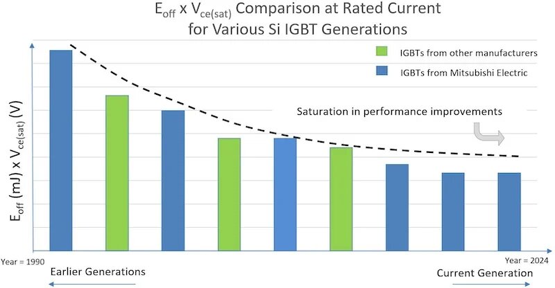
Figure 1. Eoff versus VCE(sat) Comparison for various Si IGBT Generations.
Challenge: SiC MOSFET Packaging Considerations
SiC MOSFETs can reduce switching losses because they switch much faster than Si IGBTs. However, there are challenges to achieving high switching speeds during power module operation.
Switching overvoltage: The inductive voltage overshoot during turn-off of the MOSFET (∆VDS) is a function of the stray inductance (LS) of the power module package and the rate of change of drain current (
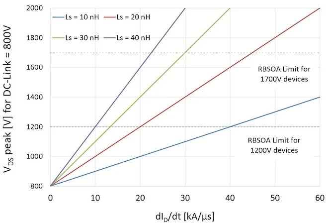
Figure 2. VDS peak versus
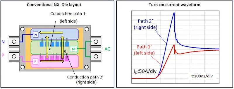
Figure 3. Internal layout of the NX module (left), turn-on current waveform for the conventional NX module (right).
It can be inferred from Figure 2 that the higher the internal inductance of the package, the lower the maximum allowable (
Internal Current Balance: The current rating of a power module depends on the number of individual chips that can be connected in parallel within the package. It is important to maintain an even distribution of drain current between chips during static and dynamic operation. Therefore, the power module package must be designed to ensure that the current is balanced across the chips.
Form Factor Preferences and Challenges: Half-bridge Si IGBT modules with 650 V, 1200 V, or 1700 V ratings in the hundreds of amperes range are widely available in the NX package, which has established itself in the industrial power supply field for several years in the converter segment. Ideally, it would be advantageous to maintain existing power module form factors such as the established NX package. However, conventional NX packages have an internal inductance (LS ) of around 20 nH, making them unsuitable for SiC. In addition, it is clear from Fig. 3 that conventional NX packages require the Si IGBT chips to be placed along the long axis of the power module. Therefore, the dynamic equalization between the chips is not optimal and poses a challenge for the direct adoption of SiC.
Low-Inductance NX Package for SiC Adoption
The internal layout of the NX package has been modified for SiC adoption. Figure 4 shows the internal cross-section of the modified NX package.
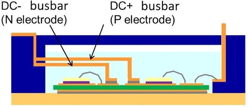
Figure 4. Internal cross-section of the modified NX package for SiC adoption.
The DC+ and DC- busbars are arranged in a "laminated structure" as close to each other as possible (separated by an insulating layer) to maximize magnetic field compensation. In addition, the DC+ and DC- busbars are bonded directly to the substrate, avoiding additional stray inductance through bonding wires to the terminals. In addition, the chips are not placed along the long axis of the module (as is the case with conventional NX designs using Si IGBTs). An optimized circuit pattern (Figure 5) has been developed for optimal current sharing between the different chips. The internal inductance of the modified low-inductance NX module was measured to be 9 nH. This is a reduction in parasitic inductance of about 47% compared to a conventional NX power module.
The NX SiC modules have been released in 1700V/600A ratings (FMF600DXE-34BN) and 1200V/600A ratings (FMF600DXE-24BN). Both devices utilize a half-bridge topology (two-in-one configuration). The power modules include ceramic substrates (AlN substrates) and are encapsulated in silicone. The power modules are based on Mitsubishi's second-generation SiC chip technology.
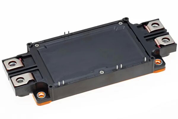
Figure 6. A photo of the NX SiC module.
Performance Benchmarking
To understand the performance improvement using the modified SiC NX module, consider the following items for benchmarking:
-Impact of the modified NX package (compared to the legacy NX package)
-Benchmarking the performance of SiC MOSFET chip technology itself (compared to Si IGBT technology)
Item 1 can be analyzed using the trade-offs shown in Figure 7 - induced voltage overshoot (VDS [V] for SiC MOSFETs and VCE [V] for IGBTs) and turn-off switching energy (Eoff [mJ/Pulse]). Considering the operating conditions DC-Link = 1000V, IC (or ID) = 600A, Tvj = 150°C, the following inferences can be drawn from Fig. 7
a) Legacy NX package: The red curve represents the VCE [V] of a 7th generation 1700V Si IGBT and a 1700V 2nd generation SiC MOSFET considering a legacy NX package (LS = ~ 20nH). The use of SiC MOSFETs in the same (conventional) package achieves lower turn-off losses ( Eoff ); however, the induced voltage overshoot cannot be maintained within the RBSOA (Reverse Bias Safe Operating Area) with sufficient safety margin.
b) Improved low-inductance NX package: The blue curve shows the V DS of a 1700V SiC MOSFET considering the improved low-inductance NX package. It can be seen that RBSOA can be maintained within safe limits without affecting Eoff.. Since LS = 9nH, a lower turn-off gate resistance can be selected.
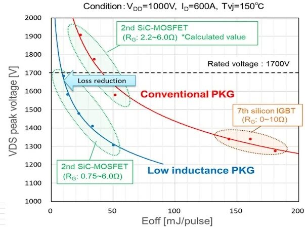
Figure 7. VDS peak versus Eoff for 2nd gen SiC considering the conventional NX package and the new low inductance NX package. 7th gen Si IGBT performance is included for reference.
Item 2 can be analyzed using Figure 8, which shows a comparison of power loss and junction temperature for a seventh-generation 1700 V Si IGBT (in a conventional NX package) and a second-generation SiC MOSFET (in a conventional and low-inductance package. NX package). The conclusion from Figure 8 is that power loss can be reduced by 72% compared to Si IGBT modules by using improved low inductance SiC MOSFETs while maintaining the NX package profile. As a result, the frequency of switching can be 5 times higher (enabling significant filter optimization) while keeping the maximum junction temperature below the maximum specified value.
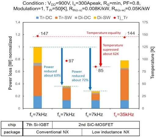
Figure 8. Normalized power loss for 7th gen Si IGBT and 2nd gen SiC considering the conventional and the new low inductance NX package.
Better Power Loss Performance
In order to maintain a competitive edge and save costs for the end user, a certain level of efficiency and compactness becomes beneficial for every power conversion application. Each generation of Si IGBTs has successfully replaced the previous generation with better power loss performance. As Si IGBT technology reaches saturation, SiC MOSFETs become increasingly attractive. The final technology frontier in the complete transition from Si to SiC is the form factor of power modules utilizing Si IGBTs. Mitsubishi Electric's improved low-inductance NX package and second-generation SiC MOSFETs are designed to address this issue and provide a viable solution for a variety of power conversions.
More about SiC can be found here.