FEATURES
256-position
End-to-end resistance 5 kΩ, 10 kΩ, 50 kΩ, 100 kΩ
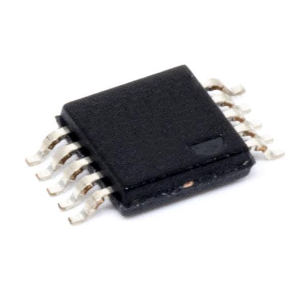
Compact MSOP-10 (3 mm × 4.9 mm) package
Pin selectable SPI/I2C compatible interface
Extra package address decode pin AD0
Full read/write of wiper register
Power-on preset to midscale
Single supply 2.7 V to 5.5 V
Low temperature coefficient 45 ppm/°C
Low power, IDD = 8 μA
Wide operating temperature −40°C to +125°C
SDO output allows multiple device daisy-chaining
Evaluation board available
APPLICATIONS
Mechanical potentiometer replacement in new designs
Transducer adjustment of pressure, temperature, position,
chemical, and optical sensors
RF amplifier biasing
Gain control and offset adjustment
GENERAL DESCRIPTION
The AD5161 provides a compact 3 mm × 4.9 mm packaged
solution for 256-position adjustment applications. These
devices perform the same electronic adjustment function as
mechanical potentiometers or variable resistors, with enhanced
resolution, solid-state reliability, and superior low temperature
coefficient performance.

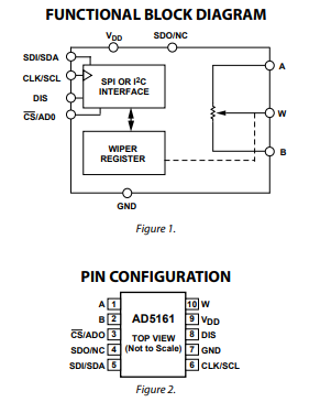
The wiper settings are controllable through a pin selectable SPI
or I2
C compatible digital interface, which can also be used to
read back the wiper register content. When the SPI mode is
used, the device can be daisy-chained (SDO to SDI), allowing
several parts to share the same control lines. In the I2
C mode,
address pin AD0 can be used to place up to two devices on the
same bus. In this same mode, command bits are available to
reset the wiper position to midscale or to shut down the device
into a state of zero power consumption.
Stresses at or above those listed under Absolute Maximum Ratings may cause permanent damage to the product. This is a stress rating only; functional operation of the product at these or any other conditions above those indicated in the operational section of this specification is not implied. Operation beyond the maximum operating conditions for extended periods may affect product reliability.
THEORY OF OPERATION
The AD5161 is a 256-position digitally controlled variable
resistor (VR)1
device.
An internal power-on preset places the wiper at midscale during
power-on, which simplifies the fault condition recovery at power-up.
PROGRAMMING THE VARIABLE RESISTOR
Rheostat Operation
The nominal resistance of the RDAC between terminals A and
B is available in 5 kΩ, 10 kΩ, 50 kΩ, and 100 kΩ. The final two
or three digits of the part number determine the nominal resistance
value, e.g., 10 kΩ = 10; 50 kΩ = 50. The nominal resistance (RAB) of
the VR has 256 contact points accessed by the wiper terminal,
plus the B terminal contact. The 8-bit data in the RDAC latch is
decoded to select one of the 256 possible settings. Assume a 10 kΩ
part is used, the wiper’s first connection starts at the B terminal
for data 0x00. Since there is a 60 Ω wiper contact resistance, such
connection yields a minimum of 60 Ω resistance between
Terminals W and B. The second connection is the first tap point,
which corresponds to 99 Ω (RWB = RAB/256 + RW = 39 Ω + 60 Ω)
for data 0x01. The third connection is the next tap point,
representing 177 Ω (2 × 39 Ω + 60 Ω) for data 0x02 and so on. Each
LSB data value increase moves the wiper up the resistor ladder
until the last tap point is reached at 9961 Ω (RAB − 1 LSB + RW).
Figure 42 shows a simplified diagram of the equivalent RDAC
circuit where the last resistor string will not be accessed;
therefore, there is 1 LSB less of the nominal resistance at full
scale in addition to the wiper resistance.

Operating from a 2.7 V to 5.5 V power supply and consuming
less than 5 μA allows for usage in portable battery-operated
applications.
The general equation determining the digitally programmed
output resistance between W and B is
WB AB RR W
D DR +´=
256 )( (1)
where D is the decimal equivalent of the binary code loaded in
the 8-bit RDAC register, RAB is the end-to-end resistance, and
RW is the wiper resistance contributed by the on resistance of
the internal switch.
In summary, if RAB = 10 kΩ and the A terminal is open circuited,
the following output resistance RWB will be set for the indicated
RDAC latch codes.
LAYOUT AND POWER SUPPLY BYPASSING
It is a good practice to employ compact, minimum lead length
layout design. The leads to the inputs should be as direct as
possible with a minimum conductor length. Ground paths
should have low resistance and low inductance.
Similarly, it is also a good practice to bypass the power supplies
with quality capacitors for optimum stability. Supply leads to
the device should be bypassed with disc or chip ceramic
capacitors of 0.01 μF to 0.1 μF. Low ESR 1 μF to 10 μF tantalum
or electrolytic capacitors should also be applied at the supplies
to minimize any transient disturbance and low frequency ripple
(see Figure 49). Note that the digital ground should also be
joined remotely to the analog ground at one point to minimize
the ground bounce.
