Scan and BIST belong to the two technologies in the DFT category. The essence is still design, because these two technologies will actually generate hardware circuits in the chip, but they are not any functions, and they are specifically for testing.
Scan Design
Scan technology was first proposed by Kobayashi et al. Its advantage is that the basic principle is that sequential circuits can be modeled as a combinational circuit network.
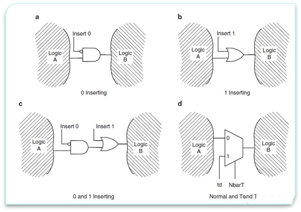
The design goal of Scan design is to be able to improve controllability and observability.
By inserting some extra hardware circuitry between logic A and logic B, it is possible to observe & control the value passed from logic A to logic B.
scan is divided into two steps:
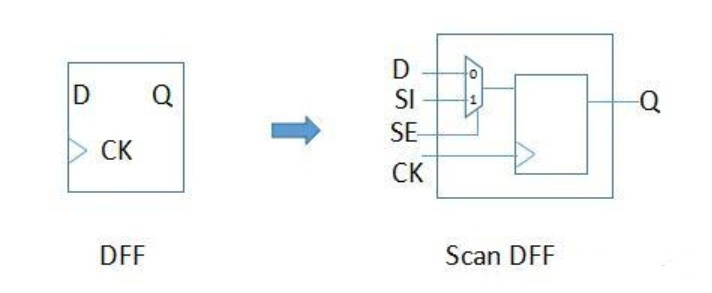
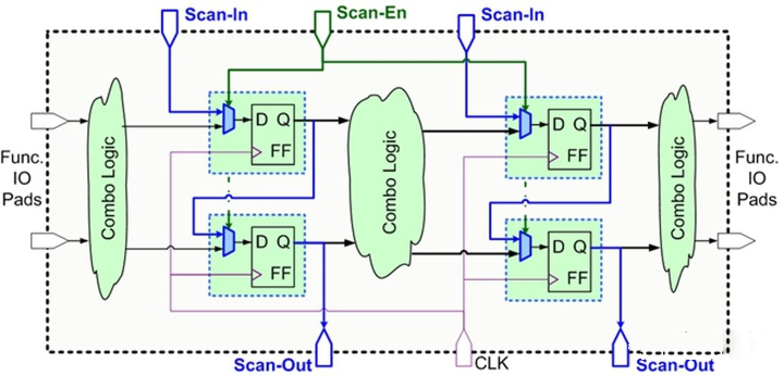
1. Scan replacement: Replace the ordinary DFF with a Scan DFF. The following figure is a mux-D DFF. You can see that there is an additional SI, SE, and a mux.
When the value of the SE terminal is 0, the circuit works in a normal functional state and can latch the value of the D terminal; when SE is 1, the circuit works in the so-called scan mode and latches the value of SI.
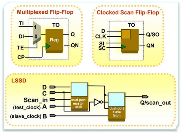
There are three common scan cells:
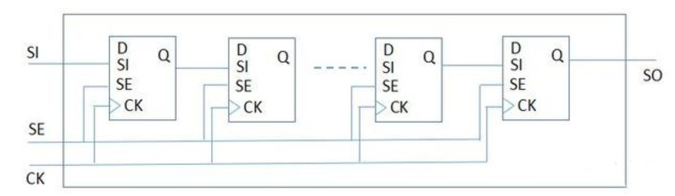
2. Scan stitching: Scan stitching is to connect the Q and SI of the Scan DFF obtained in the previous step to form a scan chain. On the top layer of the chip, there are global SE signals, and scan chain input and output signals: SI and SO. Through the continuous action of the scan chain, the problem can be transformed from testing complex sequential circuits to testing combinational circuits.
In actual design, these two steps are completed by EDA tools.
The above two pictures only have sequential units, and we will put the combinational logic in.
Before scan
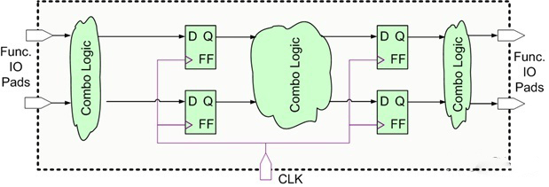
After scan insertion
Scan test steps:
1. Set Scan-En to 0, then the circuit works in normal state (function mode), and scan insertion has no effect on the normal function of the circuit.
2. Set Scan-En to 1, then enable the clock to drive the register, input the test data at the Scan-In terminal, and then observe at the output terminal Scan-Out. This method can test Flip-Flop.
3. When testing the combinational logic, set Scan-En to 1, then enable the clock to drive the register, input the test data at the Scan-In terminal, and after two clock cycles, the data will be sent to the input terminal of the combinational logic.
4. Then set Scan-En to 0, the clock beats, and the output value of the combinational logic will be sent to the register on the right.
5. Set Scan-En to 1, and the scan chain works in shift mode. At this time, the output value of the combinatorial logic can be shifted and compared with the expected value.
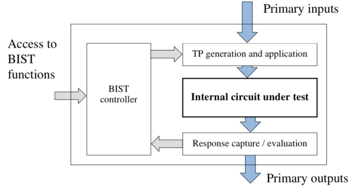
BIST -- built-in self-test
The built-in self-test (BIST) design technology adds some additional self-test circuits to the design of the chip, and only needs to apply the necessary control signals from the outside to check the circuit under test by running the built-in self-test hardware and software. defects or malfunctions. Different from scan design, built-in self-test can simplify the test steps and does not require expensive test instruments and equipment (such as ATE equipment), but it increases the complexity of chip design.
BIST can be roughly divided into two categories: Logic BIST (LBIST) and Memory BIST (MBIST)
LBIST is usually used for testing. Generally, a pseudo-random test pattern generator is used to generate input test patterns, which are applied to the internal mechanism of the device; and (MISR) is used as an output signal generator. MBIST is only used for memory testing, a typical MBIST contains test circuits for loading, reading and comparing test patterns. Currently there are several MBIST algorithms commonly used in the industry, such as "March", March-C, and MATS+ algorithms.
Another relatively rare BIST is called Array BIST, which is a kind of MBIST and is specially used for self-testing of embedded memory. Analog BIST, is used for self-testing. BIST technology is becoming an alternative to high-priced ATE, but BIST technology cannot completely replace ATE at present, and they will coexist for a long time in the future.
Scan and BIST are two very important technologies in chip testability design, and they are also necessary skills for a DFT engineer.