Overview
In this article, discuss the process of connecting ADS1115 16-bit ADC module with ESP32. The ADS1115 breakout board is a high-resolution analog-to-digital converter (ADC) that can be used in various microcontrollers, including Arduino, STM32, and ESP8266/32. The ADS1115 has a higher 16-bit resolution and provides Excellent performance. The ESP32 is a powerful microcontroller with built-in Wi-Fi and Bluetooth capabilities, making it ideal for IoT applications, has a built-in 12-bit ADC, which provides higher performance than the 10-bit ADC on the Arduino board resolution. The smallest voltage the ESP32 can measure is 3.3V / 4096 = 0.0008V (or 0.8mV), while the ADS1115 can measure down to 5V / 65536 = 0.000076V (76uV). The ADS1115 is therefore an excellent choice for precise voltage measurements.
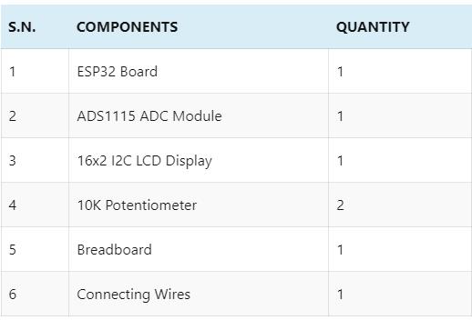
Material list
To understand the ADS1115 ADC module used with ESP32, we need the following elements:
ESP32 ADC pinout and accuracy
The ESP32 is a powerful microcontroller with integrated Wi-Fi and Bluetooth capabilities. It has several analog-to-digital converter (ADC) pins that can be used to measure an analog signal and convert it to a digital value. ESP32 has two ADCs, ADC1 and ADC2, with a total of 18 available ADC channels.
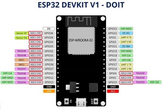
ADC1 has 8 channels (GPIO32 to GPIO39)
ADC2 has 10 channels (GPIO0, GPIO2, GPIO4, GPIO12 to GPIO15 and GPIO25 to GPIO27)
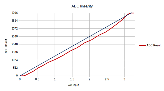
Precision: The ESP32's ADCs have 12-bit resolution, which means they can represent an analog signal using 4096 discrete levels. However, due to internal noise and non-linear characteristics, the effective resolution is usually around 10-11 bits.
To improve the accuracy of ADC readings on the ESP32, you can:
Calibration is performed using the built-in Hall sensor.
Implement oversampling and averaging to reduce noise.
For better stability is to use an external voltage reference.
If higher accuracy is required, use an external ADC module such as the ADS1115.
The ADC2 channel is shared with the Wi-Fi function, so if you are using Wi-Fi, it is best to use the ADC1 channel to avoid potential conflicts or interference with ADC readings.
ADS1115 chip
The ADS1115 is a precision, low-power, 16-bit, I2C-compatible analog-to-digital converter IC.
Features of ADS1115
16-bit resolution
Four-channel single-ended or two-channel differential input
I 2 C protocol interface
Programmable Comparator
wide range of supply
low current consumption
Continuous Conversion Mode
Programmable Data Rate
Programmable Comparator
single cycle stability
Internal Low-Drift Voltage Reference
internal oscillator
wide operating temperature range
Available in Ultra-Small X2QFN Package
ADS1115 Pin Configuration
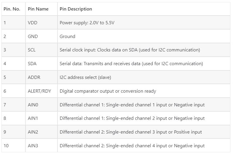
The figure below shows the pin configuration of the ADS1115 chip.
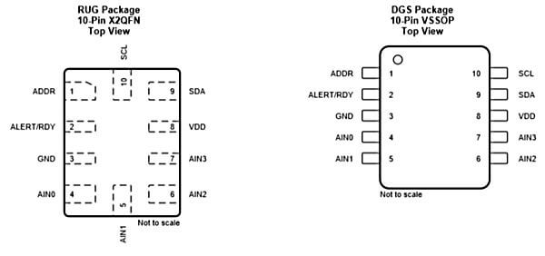
Pin 1 is the ADDR pin that selects the I2C address for the chip.
Pin 2 is the ALERT/READY pin used as a data ready and ALERT signal.
Pin 3 is the GND terminal.
Pins 4, 5, 6 and 7 are the four ADC input pins. We can use these pins as four (4) single-ended inputs or two (2) differential inputs.
Pin 8 is a positive supply pin that accepts 2.0 V to 5.5 V
Pins 9 and 10 are the terminals for the I2C interface, SCL and SDA respectively.
ADS1115 Functional Block Diagram
The functional diagram of the ADS1115 chip is presented below:
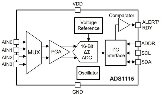
First, the multiplexer selects the input signal. This selected signal then goes to a Programmable Gain Amplifier (PGA), which can be programmed to amplify the smaller signal before conversion occurs.
Next, a 16-bit Delta Sigma converter processes the input. The converter uses its own integrated voltage reference and oscillator to measure the input signal. After the conversion is complete, the resulting data is sent to the I2C interface. Additionally, the comparator generates a signal to the external interface indicating that the converted result is available for retrieval.
Typical Connections for the ADS1115
The main I2C connections of the ADS1115 can be seen in the figure below.
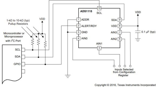
The ADS1115 is compatible with standard-mode, fast-mode, and high-speed-mode I2C controllers, enabling it to interface directly with them. The ADS1115 can be used with any microcontroller I2C peripheral, including master-only and single-master I2C peripherals.
ADS1115 Module or Breakout Board
The ADS1115 is available in X2QFN and VSSOP packages and is not suitable for prototyping. Therefore, an ADS1115 module or a breakout board is required to use it with the ESP32 or any other microcontroller.
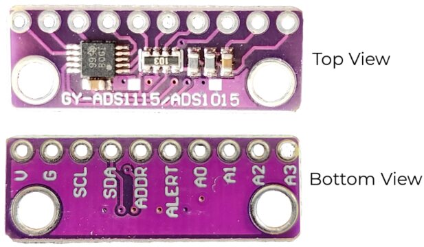
ADS1115 module pinout
The ADS1115 module has a total of 10 pins.
ADS1115 Module Schematic
The illustration shown earlier represents Adafruit's adaptation of the ADS1115 module.
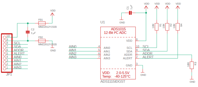
This design follows the standard connection protocol of the ADS1115 chip. It has 10K ohm pull-up resistors on the I2C and Alert pins, and a 1uF capacitor between the VDD and GND pins as a decoupling capacitor.
Connect ADS1115 module with ESP32
The ESP32 wiring diagram for connecting the ADS1115 ADC module is very simple.
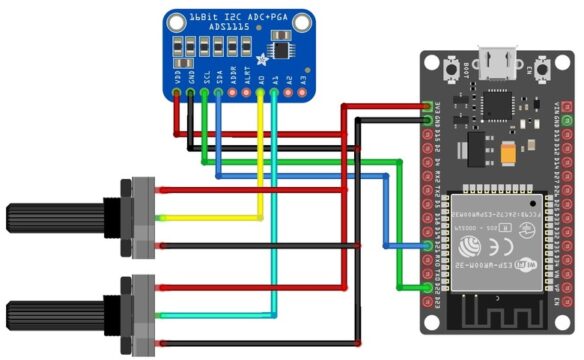
Connect the GND and VDD pins of the module to the GND pin and 3.3V of the ESP32 respectively. Next connect ADS1115 I2C pins (SDA and SCL) to ESP32 I2C pins (SDA=GPIO21 and SCL=GPIO22). The ADDR pin of the chip should be connected to VDD, SDA or SCL depending on which address you want to use 0x49, 0x4A or 0x4B. Note that the ADDR pin is pulled down to ground by a 10K resistor.
If you want to use the ALERT/READY pin of the ADS1115 module, it must be connected to an ESP32 digital pin. This pin serves two purposes. First, you can use it as an interrupt-driven transition, as a data-ready signal. Second, you can use it with a programmable output comparator to detect transition thresholds. In this case, it is used as an alarm signal.
The ADS1115 has four ADC outputs, A0, A1, A2, and A3, which means you can connect up to four analog sensors to the module. For example, to test the module reading, a potentiometer can be used, which you should connect according to the circuit diagram provided above.
For more information, please click to view the official website!