Step 1: Fabricate silicon wafers.
The raw material for making silicon wafers is our most common sand. The main component of the sand is silicon dioxide. The sand is purified to obtain elemental silicon, and then a single crystal silicon ingot is obtained by the Czochralski method. First, cut off both ends of the silicon ingot. , and then cut into several sections for rolling grinding, the purpose is to make the single crystal silicon rod reach the standard diameter.
Next, the X-ray method is used to determine the crystal orientation of single crystal silicon, cut off the reference surface, and then cut the silicon wafer based on the reference surface. After obtaining the preliminary wafer, the cut silicon wafer should be chamfered, Grind to make the surface flat and smooth, otherwise it will be difficult to carve the correct circuit on it.
After grinding, chemical etching liquid is used to remove the damage during the grinding process, and finally polishing liquid is used for polishing. After passing the inspection, it can be handed over to the production line for manufacturing.
Step 2: Deposition (Steps 2 to 7 are processes that need to be repeated many times).
Thin film deposition is to deposit a thin film of material on the surface of the wafer. The deposited material may be conductors, semiconductors and insulators. Common thin films include silicon dioxide thin films, polysilicon thin films, silicon nitride thin films, metal and compound thin films, etc.
Commonly used deposition methods are Chemical Vapor Deposition, CVD and Physical Vapor Deposition, PVD. CVD is a process method in which the vapor of the gaseous reactant or liquid reactant constituting the thin film material is introduced into the reaction chamber at a reasonable flow rate, and a chemical reaction occurs on the surface of the substrate to deposit a film.
Physical vapor deposition refers to a process in which a material source (solid or liquid) is vaporized into gaseous atoms or molecules, or partially ionized into ions, and transferred to the surface of a silicon substrate to form a thin film under vacuum conditions.
Compared with CVD, PVD has the advantages of simple process principle, low temperature required for the process, and can be used to prepare various thin films. The disadvantage is that step-coverage, adhesion, and compactness are not as good as CVD films. Common types of PVD include sputter coating, vacuum evaporation, plasma coating, etc.
Step 3: Photolithography.
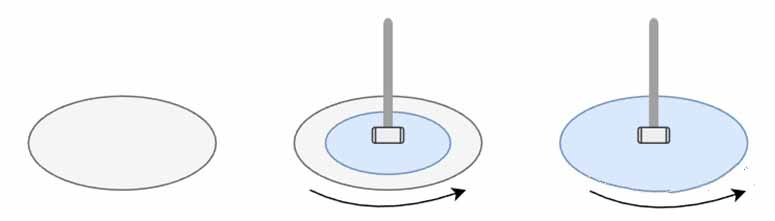
It is also the most important step in the entire manufacturing process. Before photolithography, the photoresist should be evenly coated on the wafer. Usually, the photoresist adopts the method of spin coating, that is, while rotating and smearing, to ensure the uniformity of the photoresist.
Put the photoresist-coated wafer into the lithography machine, the DUV or EUV light emitted by the light source of the lithography machine passes through the reticle, and the circuit structure pattern on the reticle is reduced and focused on the photoresist layer. After receiving light, the light-receiving area will undergo chemical changes, and the circuit pattern on the mask will be imprinted on the photoresist layer. This step is called exposure.

Step 4: Etch.
Etch is the process of using chemical or physical methods to selectively remove unwanted material from the surface of a silicon wafer after the photolithography step, leaving only a 3D circuit diagram.
The etching method mainly includes wet etching and dry etching. Wet etching refers to using the chemical reaction between the chemical solution and the pre-etching material to remove the part that is not masked by the masking film material to achieve the purpose of etching.
Dry etching is a technology that uses plasma chemical activity to etch thin films. Dry etching includes Suptter Etching, Plasma Etching, Reactive Ion Etching, and RIE.
The etching process takes plasma etching as an example. The particles in the plasma are used to hit the silicon dioxide film layer to achieve the purpose of removing the excess oxide layer.
Step 5: Measurement and testing.
After the etching, the wafer should be measured and inspected to ensure that there are no errors. If the test result is not as expected, it should be fed back to Etch or the etching step for further optimization and adjustment.
Step 6: Ion implantation.
Ion implantation means that the atoms to be doped (such as III, V group elements) are accelerated and injected into a specific area of the wafer under the action of a strong electric field, and then annealing, activating impurities, repairing lattice damage and other steps are carried out. The desired impurity concentration is obtained, and finally an N region or a P region is formed.
Step 7: Interconnect.
A technology in which each independent component in the same chip is connected to a circuit module with a certain function in a certain way. The metal materials used in the interconnection process need to have the characteristics of low resistivity, good thermochemical stability, good resistance to electromigration, easy deposition and etching, and low price.
In the early days of integrated circuit development, the aluminum interconnect process was mainly used, but copper has been widely used because of its lower resistivity and better resistance to electromigration than aluminum.
The six steps, from thin film deposition to interconnection, are repeated dozens or even hundreds of times throughout the manufacturing process. Each time, a layer of circuits is engraved on the wafer to form a complete chip.
Step 8: Testing and packaging.
After all the above steps are completed, the whole wafer is ground, polished, etc., and then tested and packaged, and qualified chips can be delivered from the factory!