PCB design is the premise and foundation of SMT manufacturing. The quality and accuracy of PCB design directly affect the efficiency and quality of SMT manufacturing. So how do we design better PCBs?
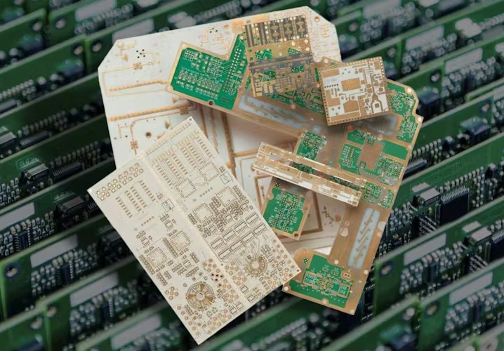
Designing a better PCB is a complex and comprehensive process that requires comprehensive consideration of multiple factors, from circuit function and performance requirements to PCB layout, circuit routing, material selection, manufacturing process and other aspects. Here are some detailed points to consider when designing a better PCB:
1. Analysis of circuit function and performance requirements:
Before PCB design, you first need to understand the functional requirements and performance indicators of the circuit. This includes signal frequency, power consumption, operating temperature range, noise requirements, etc.
Based on these requirements, determine the number of layers, component layout, circuit routing planning, etc. required for the PCB.
2. PCB size and shape design:
Determine the size and shape of the PCB based on the circuit function and mechanical structure. This includes the board’s length, width, thickness, etc.
Taking into account the installation space limitations of the PCB, ensure that the PCB can completely accommodate all components and traces.
3. Component layout design:
Reasonably arrange the location of each component according to circuit function and performance requirements. It includes chips, resistors, capacitors, connectors, etc.
Try to reduce the mutual interference between components, especially the interference between high-frequency and low-frequency signals.
4. Power supply and ground wire planning:
Analyze the power requirements of the circuit and determine the location and routing plan of the power supply lines.
Make sure ground and power traces are short and straight to reduce voltage drop and power loss.
5. Tracing and wiring design:
Design reasonable circuit routing based on component layout and circuit function requirements. This includes signal wires, power wires, ground wires, etc.
Technologies such as differential pairs and coaxial lines are used to reduce crosstalk and mutual interference between signal lines.
6. Layered wiring design:
Select the appropriate number of PCB layers based on the complexity and performance requirements of the circuit. Multi-layer PCB design can reduce signal interference and improve signal integrity.
Distribute different signal layers, power layers, and ground layers on different levels to reduce electromagnetic interference and improve electromagnetic compatibility.
7. Heat dissipation design:
For components with large power consumption, design appropriate heat dissipation structures, such as heat sinks, heat dissipation holes, etc., to improve the heat dissipation effect.
Consider the material and thickness of the PCB board and choose a material that can dissipate heat well to ensure that the operating temperature of the components is within a safe range.
8. Material selection:
Select the appropriate PCB board material based on circuit function and performance requirements. Commonly used materials include FR-4, high-frequency materials, metal substrates, etc.
Consider the surface treatment of the PCB board, such as tin spraying, lead spraying, etc., to improve the welding quality and circuit stability.
9. Manufacturing process and cost considerations:
During the PCB design process, the feasibility and cost-effectiveness of the manufacturing process are taken into consideration. Avoid overly complex designs to reduce manufacturing and maintenance costs.
Communicate with PCB manufacturers to understand their manufacturing processes and requirements to ensure that PCB design meets manufacturing requirements.
Stencil printers, pick and place systems, and reflow ovens are all important pieces of equipment when it comes to the PCB manufacturing process. They play a key role in different stages of PCB manufacturing.
Template Printer:
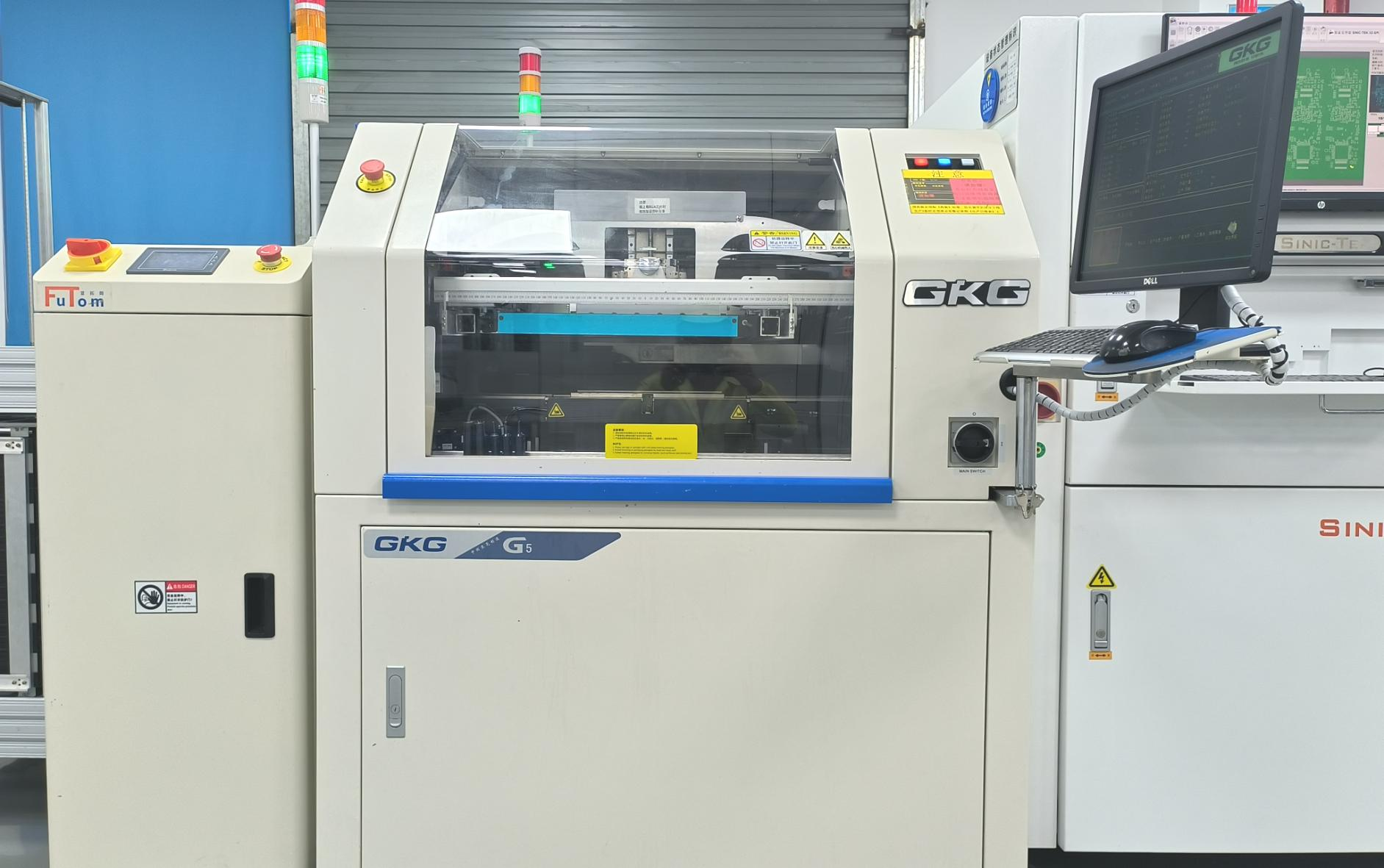
A stencil printer is used to precisely print solder paste onto the pads of a PCB. It works by squeezing solder paste through a stencil onto the surface of the PCB, forming a layer of solder paste on the pads. The accuracy and stability of the stencil printer are critical to welding quality. Typically, stencil printers use special stencils with apertures and openings designed to correspond to the pads to ensure correct solder paste distribution and thickness.
The picture shows Solder Paste Printer.
Pick and Place System:
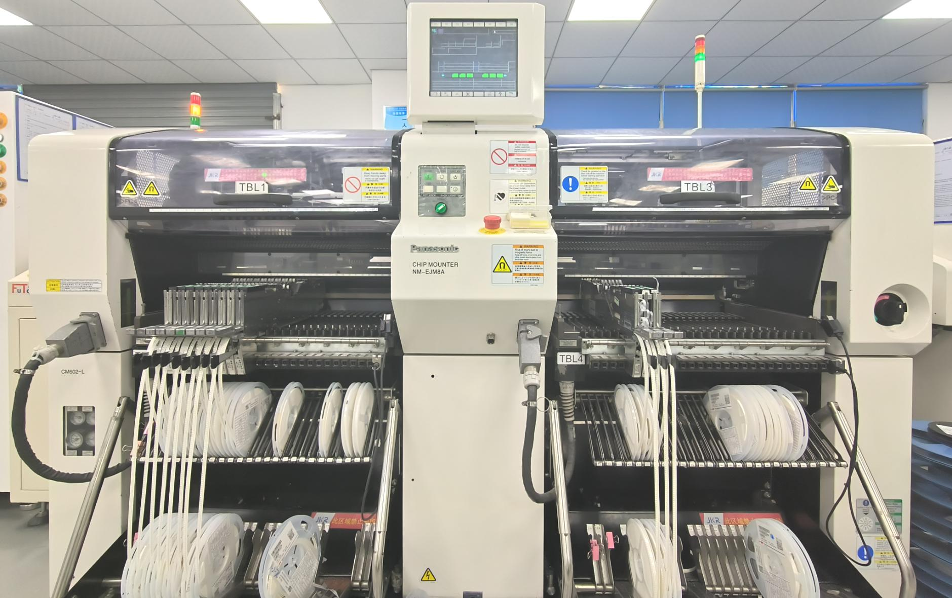
Pick and place systems are used to transfer PCB boards from one workstation to another and perform pick and place operations at different stages in the PCB manufacturing process. It automates the movement and positioning of PCBs, improving production efficiency and accuracy. Pick and place systems are usually used in conjunction with other equipment, such as pick and place machines, testing equipment, etc., to achieve automated control of the entire production process.
The picture shows the Pick and Place Machine.
Reflow soldering furnace:
Reflowing soldering furnace are used to solder components onto PCB boards. After the patch is completed, the PCB board will pass through the reflowing soldering furnace and pass through different areas such as preheating zone, soldering zone and cooling zone to achieve the soldering process. In the preheating zone, the PCB board will gradually be heated to the soldering temperature; in the soldering zone, the solder will melt and form a reliable soldering connection with the pads and components; in the cooling zone, the soldering connection will gradually cool and solidify. The temperature control and transfer speed of the reflow oven are critical to soldering quality and product stability.
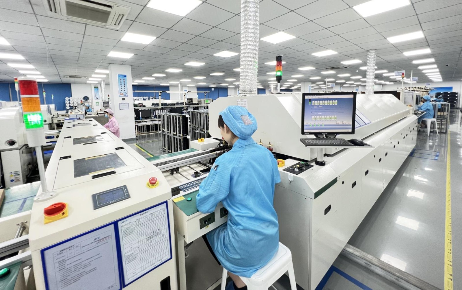
The picture shows the Reflow Soldering Oven.
During the PCB manufacturing process, these devices are often used together to form a complete production line. The stencil printer is responsible for printing solder paste, the pick and place system is responsible for transporting and positioning the PCB board, and the reflow oven is responsible for soldering components to the PCB board. By effectively organizing and managing these devices, an efficient and stable PCB manufacturing process can be achieved.
10. Simulation and verification:
Use electromagnetic simulation tools, such as SPICE, HyperLynx, etc., to conduct simulation analysis on PCB design and evaluate its performance and stability.
Conduct prototype verification and ensure that the PCB design meets expected performance and functional requirements through actual testing and debugging.
11. Standards and specifications comply with:
Follow relevant standards and specifications in the electronics industry, such as IPC standards, to ensure that PCB design complies with industry standards and requirements.
Consider electromagnetic compatibility (EMC) and electromagnetic interference (EMI) issues in PCB design to meet international electromagnetic compatibility testing requirements.
By comprehensively considering the above aspects, designing a better PCB can improve the performance, reliability and stability of the circuit, while reducing manufacturing costs and maintenance costs, thereby meeting the needs of various application scenarios.
If you have any needs for SMT technology and PCB assembly, please contact us.

