The following content is to undertake the previous article, please browse Hardware circuit design (1)
Power Problem
Power design is the most important part of the entire circuit board.
This is often referred to as DC-DC (DC-DC), and there are two types of power regulator chips that are most used in DC-DC, one is called LDO (low dropout linear regulator), and the other is called PWM (Pulse Width Modulated Switching Power Supply). We often hear that PWM has high efficiency, but LDO has fast response. Why is this?
The following will involve some theoretical knowledge, but it is still very easy to understand. If you don't understand, hey, you have to check your basics.
The working principle of linear regulated power supply
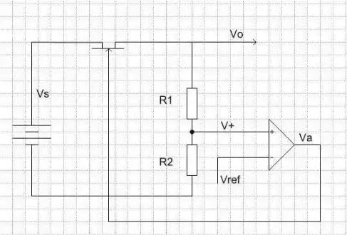
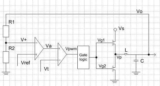
A simple schematic diagram of the internal structure of a linear regulated power supply
This is a simple schematic diagram of the internal structure of a linear regulated power supply. Our purpose is to get the low voltage Vo from the high voltage Vs. In the figure, Vo is divided by two voltage dividing resistors to get V+, V+ is sent to the positive terminal of the amplifier (we call this amplifier an error amplifier), and the negative terminal Vref of the amplifier is the internal reference level of the power supply (this reference level is constant).
The output Va of the amplifier is connected to the gate of the MOSFET to control the impedance of the MOSFET. When Va increases, the impedance of the MOSFET increases; when Va decreases, the impedance of the MOSFET decreases. The voltage drop across the MOSFET will be Vs-Vo.
Now let's see how Vo is stable. If Vo becomes smaller, then V+ will become smaller, and the output Va of the amplifier will also become smaller, which will cause the impedance of the MOSFET to become smaller, so that through the same current, the voltage difference of the MOSFET will become smaller. becomes smaller, so the Vo is lifted up to suppress the decrease of Vo. In the same way, when Vo becomes larger, V+ becomes larger, Va becomes larger, and the impedance of the MOSFET becomes larger. After the same current, the voltage difference of the MOSFET becomes larger, so the increase of Vo is suppressed.
The working principle of switching power supply
As shown in the figure above, in order to obtain Vo from the high voltage Vs, the switching power supply adopts square waves Vg1 and Vg2 with a certain duty cycle to drive the upper and lower MOS tubes. Vg1 and Vg2 are in opposite phases, Vg1 is high, and Vg2 is low. When the upper MOS tube is turned on, the lower MOS tube is turned off; when the lower MOS tube is turned on, the upper MOS tube is turned off.
As a result, a square wave voltage with a certain duty cycle is formed at the left end of L. The inductor L and capacitor C can be regarded as a low-pass filter. Therefore, after the square wave voltage is filtered, the filtered stable voltage Vo is obtained.
Vo is divided by R1 and R2 and sent to the negative terminal V+ of the first amplifier (error amplifier), the output Va of the error amplifier is used as the positive terminal of the second amplifier (PWM amplifier), and the output Vpwm of the PWM amplifier is a The square wave with a certain duty cycle is processed by the gate logic circuit to obtain two opposite-phase square waves Vg1 and Vg2 to control the switching of the MOSFET.
The positive terminal Vref of the error amplifier is a constant voltage, while the negative terminal Vt of the PWM amplifier is a triangular wave signal. Once Va is larger than the triangular wave, Vpwm is high; when Va is smaller than the triangular wave, Vpwm is low, so the relationship between Va and the triangular wave , determines the duty cycle of the square wave signal Vpwm; when Va is high, the duty cycle is low, and when Va is low, the duty cycle is high.
After processing, Vg1 and Vpwm are in the same phase, and Vg2 and Vpwm are in opposite phase; finally, the square wave voltage Vp at the left end of L is the same as Vg1. As shown below
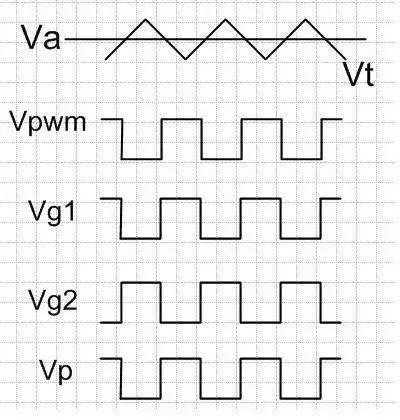
When Vo rises, V+ will rise, Va falls, and the duty cycle of Vpwm decreases. After the gate logic, the duty cycle of Vg1 decreases, the duty cycle of Vg2 increases, and the duty cycle of Vp decreases, which in turn causes Vo to decrease, so The rise of Vo will be suppressed. vice versa.
Comparison of Linear Regulated Power Supply and Switching Power Supply
After understanding the working principle of linear regulated power supply and switching power supply, we can understand why linear regulated power supply has less noise, faster transient response, but poor efficiency; while switching power supply has larger noise and transient response Slower, but more efficient.
The internal structure of the linear regulated power supply is simple, the feedback loop is short, so the noise is small, and the transient response is fast (when the output voltage changes, the compensation is fast). But because the voltage difference between input and output all falls on the MOSFET, its efficiency is low. Therefore, linear regulators are generally used in applications with small currents and high voltage accuracy requirements.
The switching power supply has a complex internal structure, many factors affecting the output voltage noise performance, and its feedback loop is long, so its noise performance is lower than that of a linear regulated power supply, and its transient response is slow. However, according to the structure of the switching power supply, the MOSFET is in two states: fully on and fully off. Except for the energy consumed by the driving MOSFET and the internal resistance of the MOSFET, all other energy is used for the output (in theory, L and C are not consumed). energy, although it is not actually the case, these consume a small amount of energy).
Some misunderstandings of high-speed signal recognition
The high speed looks at the signal edge, not the clock frequency. Generally speaking, if the clock frequency is high, the rising edge of the signal is fast, so we generally regard them as high-speed signals; but the reverse is not necessarily true. If the clock frequency is low, if the rising edge of the signal is still fast, it should be regarded as a high-speed signal. signal to handle.
According to signal theory, the rising edge of the signal contains high-frequency information (using Fourier transform, the quantitative expression can be found), therefore, once the rising edge of the signal is very steep, we should treat it as a high-speed signal, and it is likely that a rising edge will appear if the design is not good. Too slow, with overshoot, undershoot, and ringing.
Therefore, we should pay more attention to the signal bandwidth. According to the empirical formula, the relationship between bandwidth and rise time (10%~90%) is Fw * Tr = 3.5.
Oscilloscope Selection
Pay attention to the bandwidth of the oscilloscope
Many people pay attention to the sampling rate of the oscilloscope, but not the bandwidth of the oscilloscope, but often the oscilloscope bandwidth is a more important parameter. Some people think that as long as the sampling rate of the oscilloscope is more than twice the clock frequency of the signal, this is a big mistake. The reason for the mistake is a wrong understanding of the sampling theorem. The sampling theorem states that when the sampling frequency is greater than twice the maximum bandwidth of the signal, the original signal can be perfectly recovered. However, the signal that the sampling theorem refers to is a band-limited signal (the bandwidth is limited), which is seriously inconsistent with the signal in reality.
Our general digital signal is not periodic except for the clock. From a long-term perspective, its spectrum is infinitely wide. To capture high-speed signals, it cannot distort its high-frequency components too much. Oscilloscope bandwidth metrics are closely related to this. Therefore, the real concern is still that the rising edge distortion of the signal captured with the oscilloscope is within our acceptable range.
So how many high-bandwidth oscilloscopes are appropriate?
Theoretically, the signal captured by an oscilloscope with 5 times the signal bandwidth will lose less than 3% of the original signal. If more lenient losses are required, a lower end oscilloscope can be chosen. Using an oscilloscope with 3 times the signal bandwidth should suffice for most requirements, but don't forget the bandwidth of your probe.