The following will introduce how the Buck converter, one of the three most basic topologies, evolved.
Anyone who has studied electronics should know that how to get the desired voltage value (low) from a voltage (high), perhaps the easiest way is to divide the voltage through resistors, as in the following way.
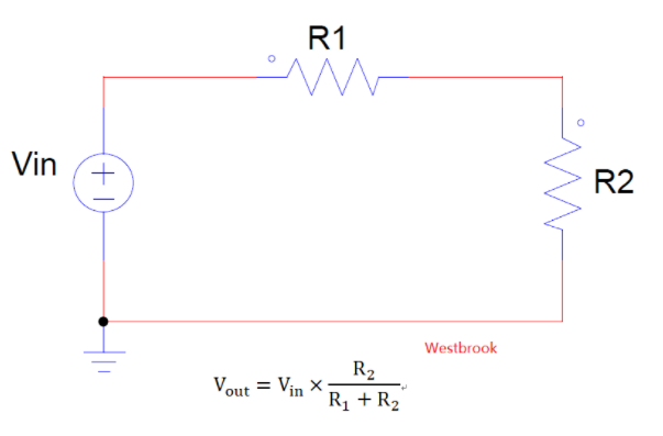
This method is the most convenient and fast, and now the general voltage sampling basically adopts this method, but what if the power is slightly larger? Since R1 and R2 are connected in series, the loss in R1 cannot be ignored. If the required voltage is much lower than the input voltage, the efficiency of the circuit will be extremely low. Try to deform the circuit, replace R1 with a triode, which is the current LDO model, as follows:

Through the modification, the original loss on R1 is transferred to the transistor Q1. Since Q1 bears the voltage difference between the input and output, the efficiency of the circuit is relatively low. In order to improve efficiency, the triode was working in a linear state before, can it be changed to a switching state? In this way, the triode only has switching loss and conduction loss, so the loss will be greatly reduced. Can be changed to the following circuit:

The working cycle time of this circuit is Ts, the conduction time is Ton, then the duty cycle is D=Ton/Ts, but in this way the output voltage is highly related to the switch state, there is an output voltage when S1 is on, and there is no output voltage when S1 is off , but the output load always requires a continuous energy supply, which is unacceptable for the output load. This requires decoupling, and the capacitor of the energy storage component is introduced at a certain position of the converter, so that even when the input terminal S1 is disconnected, the output capacitor can continue to output energy to ensure the stability of the output voltage.

If you do this, do you see what kind of effect it will bring? Since the voltage across the capacitor cannot change abruptly, when S1 is closed, a very large inrush current will be generated in the line, which will not only cause noise and EMI problems, but S1 may be damaged at this time. So it needs to limit the current, as follows:

After adding the R2 current-limiting resistor, there will be no such a large inrush current at the moment S1 is closed, but since R2 is connected in series in the main power circuit, the resistor will consume power, so that the reduced power consumption on the switch may eventually be reduced. dissipated in the added resistor. Therefore, in order to maximize the efficiency, R2 can be transformed into a reactance element. In principle, the reactance element only stores energy and does not consume energy. As we all know, the current at both ends of the inductor cannot change suddenly, so when the switch S1 is closed, the inductor It can suppress the inrush current very well without consuming energy. as follows:

This solves the surge current caused by the action of C1 when S1 is closed, but what about when S1 is disconnected? As mentioned just now, the current at both ends of the inductor cannot change suddenly. When S1 is suddenly disconnected, it is equivalent to a sudden change in the current of the inductor. Since there is no freewheeling circuit, the energy stored in the inductor will be consumed in the form of "arcing". , which creates a very large voltage spike. Therefore, in order to provide a freewheeling path for the inductor L1, a freewheeling diode needs to be added, as follows:

In this way, when S1 is suddenly disconnected, the energy of L1 will continue to flow through the diode, so we also call it a freewheeling diode. Of course, in order to improve efficiency, the freewheeling diode can be replaced with a MOSFET, as follows:

Such a synchronous Buck converter is produced. The inductor can be placed in different positions and transformed into different topological structures. Putting it at the input end is a Boost converter, and placing it at the bottom is a Buck-boost converter. Therefore, there are only these three basic converters, and many other topologies are evolutions of these three basic converters.
For example, forward is the isolated version of Buck, and flyback is the isolated version of Buck-boost.
Related Products
The NCP1529 step−down DC−DC converter is a monolithic integrated circuit for portable applications powered from one cell Li−ion or three cell Alkaline/NiCd/NiMH batteries.
The device is able to deliver up to 1.0 A on an output voltage range externally adjustable from 0.9 V to 3.9 V or fixed at 1.2 V or 1.35 V.
It uses synchronous rectification to increase efficiency and reduce external part count.
The device also has a built−in 1.7 MHz (nominal) oscillator which reduces component size by allowing a small inductor and capacitors.
Automatic switching PWM/PFM mode offers improved system efficiency.
Additional features include integrated soft−start, cycle−by−cycle current limiting and thermal shutdown protection.

Model: NCP1529ASNT1G